
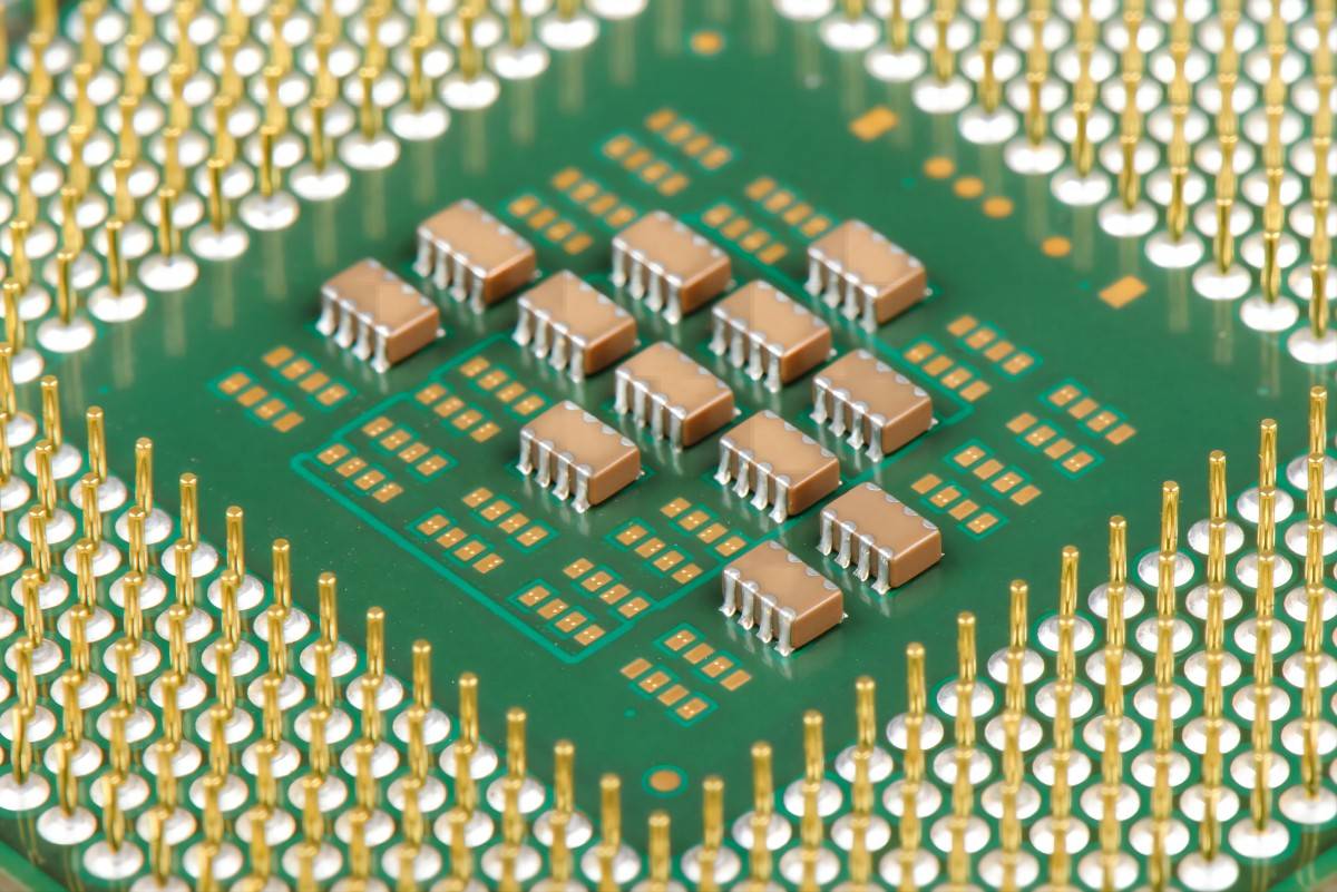
Minimum Pad Clearance PCB manufacturing
Minimum Pad Clearance PCB manufacturing, For the LED PCBs, BGA substrates. or other HDI PCBs. we will meet this small clearance PCB design. we can produce the minimum pads clearance PCBs from 2 layer to 22 layers. Minimum Pad Clearance PCBs are printed circuit boards designed with meticulous attention to the distance between conductive pads and adjacent elements. This critical parameter ensures the prevention of electrical shorts and enhances the reliability and performance of electronic devices. By adhering to specified clearance requirements during the design and manufacturing processes, these PCBs maintain signal integrity, minimize interference, and optimize functionality. Designers utilize advanced PCB design software to define and enforce clearance rules, guaranteeing compliance with industry standards and customer specifications. PCB manufacturers employ precise fabrication techniques, including photolithography and chemical etching, to achieve the desired pad clearances accurately. Quality control measures, such as automated optical inspection and rigorous testing, ensure that Minimum Pad Clearance PCBs meet stringent quality standards. Ultimately, these PCBs play a vital role in the creation of robust and dependable electronic systems across various industries.
What is Minimum Pad Clearance PCB?
Minimum pad clearance on a printed circuit board (PCB) refers to the minimum distance required between the edge of a conductive pad and other adjacent conductive elements or features on the PCB, such as traces or other pads. This clearance is crucial to prevent short circuits and ensure proper functionality and reliability of the PCB.
The minimum pad clearance requirements can vary depending on several factors, including the manufacturing process, the type of components being used, the operating voltage, and the desired reliability standards. Designers typically specify the minimum pad clearance in the PCB design rules, which are followed during the layout and manufacturing process.
Failure to adhere to minimum pad clearance requirements can lead to electrical shorts, signal interference, or even catastrophic failure of the PCB. Therefore, it’s essential for PCB designers to carefully consider and adhere to these specifications during the design process to ensure the overall functionality and reliability of the PCB.
Minimum Pad Clearance PCB manufacturing
What are Minimum Pad Clearance PCB Design Guidelines?
Minimum pad clearance PCB design guidelines are recommendations or specifications provided to PCB designers regarding the minimum allowable distance between conductive pads and other conductive elements on a printed circuit board (PCB). These guidelines ensure proper functionality, reliability, and manufacturability of the PCB. Here are some common minimum pad clearance PCB design guidelines:
- Manufacturer’s Specifications: Always refer to the manufacturer’s datasheets and design guidelines for specific recommendations regarding minimum pad clearances. Different manufacturers may have different requirements based on their manufacturing processes and capabilities.
- IPC Standards: The Institute for Interconnecting and Packaging Electronic Circuits (IPC) provides industry-standard guidelines for PCB design. IPC-2221B, “Generic Standard on Printed Board Design,” and IPC-2222, “Sectional Design Standard for Rigid Organic Printed Boards,” contain recommendations for pad clearances among other design considerations.
- Clearance from Traces: Ensure an adequate distance between pads and adjacent traces to prevent electrical shorts. This distance may vary depending on the voltage levels and potential noise or interference.
- Clearance from Copper Pours: Maintain a minimum clearance between pads and nearby copper pours to avoid unintended connections or shorts.
- Component Footprints: Use recommended footprint patterns provided by component manufacturers to determine the appropriate pad sizes and clearances for specific components.
- Design Rule Checks (DRC): Implement design rule checks in PCB design software to enforce minimum pad clearance requirements and detect violations during the design process.
- Consideration of Manufacturing Processes: Take into account the capabilities and limitations of the PCB fabrication and assembly processes. Ensure that the minimum pad clearances are feasible for the chosen manufacturing methods.
- Environmental Considerations: Consider environmental factors such as temperature variations, humidity, and vibration, which may affect the performance and reliability of the PCB over time.
- Signal Integrity:Maintain appropriate pad clearances to minimize signal distortion and interference, especially in high-speed or high-frequency circuits.
- Documentation: Document the minimum pad clearance requirements in the PCB design documentation to ensure consistency and facilitate communication with manufacturers and other stakeholders.
By following these minimum pad clearance PCB design guidelines, designers can create PCB layouts that meet electrical, mechanical, and manufacturability requirements while ensuring reliable and robust performance of the final product.
What is the Minimum Pad Clearance PCB Fabrication Process?
The minimum pad clearance in the PCB fabrication process refers to the minimum allowable distance between conductive pads and other adjacent conductive features on the PCB during manufacturing. Ensuring proper pad clearance is essential to prevent short circuits and ensure the reliability of the finished PCB. Here’s an overview of the steps involved in maintaining minimum pad clearance during PCB fabrication:
- Design Phase: PCB designers specify the minimum pad clearance requirements in the design files using PCB design software. They define the clearance rules based on factors such as the PCB’s electrical requirements, component footprints, manufacturing capabilities, and industry standards.
- Preparation of Manufacturing Data: Once the PCB design is complete, the design files are prepared for manufacturing. This includes generating Gerber files, drill files, and other necessary documentation that convey the design information to the PCB fabrication facility.
- Manufacturing Process Planning: The PCB fabrication facility reviews the design files and plans the manufacturing process accordingly. This involves selecting appropriate materials, determining the fabrication techniques, and setting up the equipment to meet the specified design requirements, including minimum pad clearance.
- Lithography and Etching: In the initial stages of PCB fabrication, a layer of photosensitive material (photoresist) is applied to the copper-clad substrate. The PCB design pattern is then transferred onto the photoresist layer using photolithography techniques. After exposure to UV light through a photomask, the unexposed areas of the photoresist are dissolved, leaving behind the desired pattern. The exposed copper is then etched away using chemical solutions, defining the conductive traces and pads on the PCB.
- Inspection and Quality Control:Throughout the fabrication process, quality control measures are implemented to ensure that the minimum pad clearance requirements are met. Automated optical inspection (AOI) systems and manual inspections are performed to verify that there are no defects or deviations from the design specifications.
- Surface Finish Application: After the conductive features are defined, the PCB may undergo surface finish processes such as electroless nickel immersion gold (ENIG), immersion tin (ISn), or hot air solder leveling (HASL). These surface finishes help protect the exposed copper surfaces and ensure good solderability during assembly.
- Final Inspection: Once the fabrication process is complete, a final inspection is carried out to verify that the PCB meets all specified requirements, including minimum pad clearance. Any deviations or defects are addressed before the PCBs are sent for assembly.
By carefully managing the fabrication process and adhering to the minimum pad clearance requirements specified in the design, PCB manufacturers ensure the reliability and functionality of the finished PCBs.
How to Manufacture Minimum Pad Clearance PCB?
Manufacturing a PCB with minimum pad clearance requires careful attention to detail throughout the fabrication process. Here are the steps involved in manufacturing a PCB with minimum pad clearance:
- Design Phase:
– Define the minimum pad clearance requirements based on factors such as component footprints, electrical requirements, and manufacturing capabilities.
– Specify the pad clearance rules in the PCB design software to ensure compliance during layout.
- Preparation of Design Files:
– Finalize the PCB design and generate the necessary design files, including Gerber files, drill files, and assembly drawings.
- Material Selection:
– Choose PCB materials that meet the design requirements and are suitable for achieving minimum pad clearance. Consider factors such as dielectric properties, thickness, and thermal conductivity.
- PCB Fabrication Process:
– Preparation: Clean the substrate material (typically fiberglass-reinforced epoxy laminate) and apply a thin layer of copper foil.
– Lithography: Apply a layer of photoresist onto the copper surface. Transfer the PCB design pattern onto the photoresist using photolithography techniques.
– Etching: Use chemical etchants to remove the exposed copper, leaving behind the desired conductive traces and pads. Ensure that the etching process achieves the minimum pad clearance specified in the design.
– Inspection: Perform visual inspections and automated optical inspections (AOI) to verify that the minimum pad clearance requirements are met and there are no defects or deviations.
– Surface Finish: Apply surface finishes such as ENIG, HASL, or immersion silver to protect the exposed copper surfaces and ensure good solderability.
- Quality Control:
– Conduct thorough quality control checks throughout the fabrication process to ensure that the minimum pad clearance is maintained and all other specifications are met.
- Final Inspection:
– Perform a final inspection of the fabricated PCBs to verify compliance with the minimum pad clearance requirements and other design specifications.
- Assembly (optional):
– If required, assemble the PCBs with electronic components using surface mount technology (SMT) or through-hole technology (THT).
- Testing:
– Test the assembled PCBs to ensure proper functionality and reliability.
By following these steps and maintaining strict adherence to the minimum pad clearance specifications throughout the manufacturing process, PCB manufacturers can produce high-quality PCBs with reliable performance.
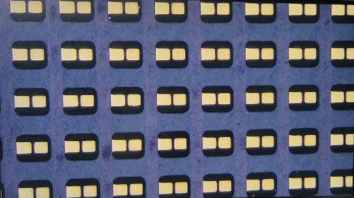
2.3Mil gap LED PCB
How much should Minimum Pad Clearance PCB cost?
The cost of manufacturing a PCB with minimum pad clearance can vary depending on several factors, including the complexity of the design, the size of the PCB, the number of layers, the chosen materials, surface finish options, and the production volume. Here are some factors that can influence the cost:
- Design Complexity: PCBs with intricate designs, dense component placement, and fine pitch components may require more advanced fabrication techniques, which can increase the manufacturing cost.
- Number of Layers: PCBs can range from single-layer to multi-layer designs. Multi-layer PCBs typically cost more due to the additional fabrication steps required.
- Materials: The choice of materials, such as substrate material and copper thickness, can affect the cost. High-quality materials that meet specific performance requirements may come at a premium.
- Surface Finish: Different surface finish options have varying costs. For example, ENIG (Electroless Nickel Immersion Gold) tends to be more expensive than HASL (Hot Air Solder Leveling).
- Production Volume: Larger production volumes generally lead to lower per-unit costs due to economies of scale. However, prototype or low-volume production runs may incur higher costs per unit.
- Turnaround Time: Expedited or quick-turn manufacturing services often come with additional fees compared to standard lead times.
- Additional Services: Additional services such as electrical testing, panelization, and conformal coating may add to the overall cost.
It’s important to obtain quotes from multiple PCB manufacturers to compare pricing and evaluate which one offers the best balance of cost, quality, and lead time for your specific requirements. Additionally, working closely with the manufacturer to optimize the design for manufacturability can help reduce costs without sacrificing quality.
What is Minimum Pad Clearance PCB Base Material?
The base material for a PCB refers to the substrate upon which the conductive traces and components are mounted. The choice of base material is critical for achieving the minimum pad clearance requirements and ensuring the overall performance and reliability of the PCB. Common base materials used in PCB manufacturing include:
- FR-4 (Flame Retardant-4): FR-4 is the most widely used substrate material for PCBs. It is made of woven fiberglass cloth impregnated with epoxy resin. FR-4 offers good electrical insulation properties, mechanical strength, and dimensional stability. It is suitable for a wide range of applications and can meet minimum pad clearance requirements effectively.
- FR-4 High Tg: FR-4 High Tg (Glass Transition Temperature) is a variant of FR-4 with a higher Tg value, typically above 170°C. This material is chosen for applications that require higher thermal stability, such as lead-free soldering processes. FR-4 High Tg can also meet minimum pad clearance requirements effectively.
- Polyimide (PI): Polyimide is a high-temperature resistant polymer often used in flexible PCBs (Flex PCBs) and rigid-flex PCBs. It offers excellent thermal stability, chemical resistance, and flexibility. Polyimide-based substrates can meet minimum pad clearance requirements and are suitable for applications with demanding environmental conditions.
- Rogers Materials: Rogers Corporation offers a range of high-performance materials specifically designed for RF/microwave applications. These materials feature low dielectric constants, low loss tangents, and excellent RF properties. They are commonly used in high-frequency PCBs and can meet minimum pad clearance requirements.
- Metal Core: Metal core PCBs use a metal substrate, typically aluminum or copper, as the base material instead of fiberglass. Metal core PCBs offer superior thermal conductivity, making them suitable for high-power applications and applications requiring efficient heat dissipation. They can meet minimum pad clearance requirements effectively.
When selecting the base material for a PCB with minimum pad clearance requirements, it’s essential to consider factors such as electrical properties, thermal properties, mechanical strength, and cost. Additionally, verifying that the chosen base material complies with relevant industry standards and specifications ensures the reliability and performance of the finished PCB.
Which company manufactures Minimum Pad Clearance PCBs?
Currently, many PCB manufacturing companies can produce PCBs that meet the minimum pad clearance requirements. Some of these well-known companies include Foxconn, JLCPCB, Nine Sunplus Systems, and Huaqiang Electronics. These companies have advanced manufacturing equipment, extensive experience, and professional technical teams to meet various PCB design requirements, including minimum pad clearance.
As a professional PCB manufacturing company, our company can also produce PCBs that meet the minimum pad clearance requirements. We have advanced production equipment and a skilled technical team to meet customers’ strict requirements for PCB quality and performance. Our manufacturing process strictly follows international standards to ensure that the produced PCBs have excellent electrical characteristics, stability, and reliability.
Our company can customize PCB designs according to customer requirements, including minimum pad clearance, complex routing rules, and special material requirements. We provide professional technical support and customization services, working closely with customers to ensure that their designs meet their application needs to the fullest extent.
Furthermore, we prioritize quality control and after-sales service. We strictly adhere to quality management systems to ensure that every PCB meets specification requirements. If customers encounter any problems during use, we provide timely technical support and after-sales service to ensure customer satisfaction.
In summary, as an experienced and professionally skilled PCB manufacturing company, we can provide customers with high-quality PCB products that meet the minimum pad clearance requirements, satisfying the needs of various application fields.
What are the 7 qualities of good customer service?
Good customer service is essential for building and maintaining positive relationships with customers. Here are seven qualities that characterize good customer service:
- Responsiveness: Good customer service involves being prompt and timely in responding to customer inquiries, concerns, and requests. Whether it’s answering phone calls, replying to emails, or addressing issues in person, being responsive shows customers that their needs are valued and prioritized.
- Empathy: Empathy involves understanding and relating to the customer’s emotions, concerns, and perspectives. Good customer service representatives demonstrate empathy by actively listening to customers, acknowledging their feelings, and showing genuine concern for their satisfaction.
- Professionalism: Professionalism encompasses maintaining a courteous, respectful, and professional demeanor when interacting with customers. This includes using appropriate language, maintaining composure, and demonstrating expertise in addressing customer inquiries and resolving issues.
- Knowledgeability: Good customer service requires having a thorough understanding of the products or services offered, as well as company policies, procedures, and processes. Knowledgeable customer service representatives can provide accurate information, offer helpful recommendations, and effectively assist customers with their needs.
- Flexibility: Flexibility involves adapting to the unique needs and preferences of each customer. Good customer service representatives are willing to accommodate special requests, explore alternative solutions, and adjust their approach to meet the customer’s expectations.
- Problem-Solving Skills: Effective problem-solving skills are crucial for resolving customer issues and concerns in a timely and satisfactory manner. Good customer service representatives are resourceful, creative, and proactive in identifying solutions, addressing root causes, and preventing recurrence of problems.
- Consistency: Consistency in delivering high-quality customer service across all interactions and touchpoints is key to building trust and loyalty with customers. Good customer service is reliable, predictable, and consistent in meeting or exceeding customer expectations every time.
By embodying these qualities, organizations can cultivate a customer-centric culture and build strong, long-lasting relationships with their customers.
FAQs (Frequently Asked Questions) about Minimum Pad Clearance PCBs
What is minimum pad clearance in PCB design?
Minimum pad clearance refers to the minimum allowable distance between the edge of a conductive pad and other adjacent conductive elements on a printed circuit board (PCB). It is crucial to prevent short circuits and ensure proper functionality of the PCB.
Why is minimum pad clearance important?
Minimum pad clearance is important to avoid electrical shorts and ensure the reliability and performance of the PCB. Proper clearance helps maintain signal integrity, prevent interference, and ensure the overall functionality of the electronic device.
How is minimum pad clearance determined in PCB design?
Minimum pad clearance is determined based on factors such as the manufacturing process, component footprints, operating voltage, and industry standards. Designers specify the clearance requirements in the PCB design rules, which are followed during layout and fabrication.
What are the consequences of not adhering to minimum pad clearance requirements?
Failure to adhere to minimum pad clearance requirements can lead to electrical shorts, signal interference, and malfunction of the PCB. This can result in the failure of the electronic device and may require costly repairs or replacements.
Can minimum pad clearance be adjusted for different components?
Yes, minimum pad clearance can be adjusted based on the requirements of different components. Designers may specify different clearance rules for components with varying sizes, voltage levels, or sensitivity to interference.
What are some common industry standards for minimum pad clearance?
Common industry standards for minimum pad clearance include those provided by the Institute for Interconnecting and Packaging Electronic Circuits (IPC), such as IPC-2221B and IPC-2222. These standards provide guidelines for PCB design and manufacturing.
How can I ensure that minimum pad clearance requirements are met in my PCB design?
To ensure that minimum pad clearance requirements are met, it is important to use PCB design software that allows you to specify clearance rules and perform design rule checks (DRC). Additionally, working closely with PCB manufacturers and following best practices in layout and fabrication can help ensure compliance with clearance requirements.