
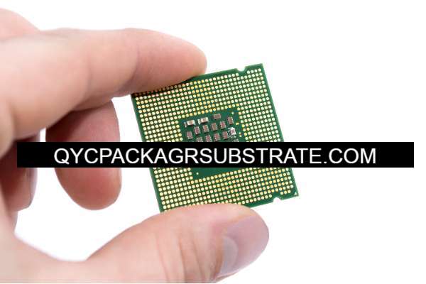
Minimum Spacing PCB Manufacturer
Minimum Spacing PCB Manufacturer,Minimum Spacing PCB refers to printed circuit boards designed with extremely close spacing between conductive traces and components. This design approach allows for compact and densely packed electronic assemblies, crucial for achieving miniaturization in modern electronics. Minimum Spacing PCBs require precise manufacturing techniques to ensure that electrical signals do not interfere or cross-talk between adjacent traces. They are utilized in high-density applications such as smartphones, tablets, and wearable devices, where space efficiency is paramount. These PCBs enable efficient routing of signals while maintaining signal integrity, contributing to the overall performance and reliability of electronic products requiring compact yet high-functioning designs.
What is a Minimum Spacing PCB?
A Minimum Spacing PCB (Printed Circuit Board) refers to the smallest allowable distance between any two conductive elements or components on the board. These elements could be traces, pads, or vias. The spacing is critical because it ensures that electrical signals do not interfere with each other or cause unintended short circuits.
Designing a PCB with minimum spacing involves considering various factors such as voltage levels, signal integrity, electromagnetic interference (EMI), and manufacturing capabilities. Smaller spacing allows for denser packing of components and more compact designs, which is crucial for modern electronics where miniaturization is often a priority.
However, reducing spacing also increases the risk of signal crosstalk, noise, and potential manufacturing defects like solder bridges. Therefore, designers must balance between achieving the smallest possible spacing and ensuring reliable functionality and manufacturability of the PCB.
Advanced PCB design software tools help engineers optimize spacing by considering electrical characteristics, thermal management, and mechanical constraints. This ensures that the final PCB layout meets both electrical and physical requirements for the intended application.
Minimum Spacing PCB Manufacturer
What are the Minimum Spacing PCB Design Guidelines?
Minimum spacing PCB design guidelines outline the rules and recommendations for maintaining safe distances between various conductive elements on a printed circuit board. These guidelines ensure reliable operation, prevent electrical interference, and facilitate manufacturability. Here are key aspects typically covered in minimum spacing guidelines:
- Clearance between Traces: This refers to the minimum distance between two adjacent traces. It prevents electrical shorts and crosstalk between signals. Typical values range from 6 mils (0.006 inches) for controlled impedance traces to 8 mils or more for general-purpose traces.
- Clearance from Traces to Pads/Vias: Pads and vias must maintain adequate spacing from nearby traces to prevent solder bridges during assembly and ensure electrical isolation. Guidelines often specify minimum distances based on trace width and pad/via diameter.
- Clearance from Components: Components such as resistors, capacitors, and integrated circuits require specified spacing from nearby traces and other components to avoid interference and ensure proper soldering.
- Edge Clearance:The distance between any conductive feature (trace, pad, via) and the edge of the PCB is critical to prevent mechanical stress during handling and assembly. Edge clearance guidelines ensure reliability and prevent damage.
- Minimum Annular Ring: This is the copper area around a via pad or component pad that connects the pad to the trace or plane. It must be sufficient to maintain electrical conductivity and mechanical strength. Guidelines typically specify minimum annular ring widths.
- Spacing for High-Voltage Traces: Traces carrying high voltages require larger spacings to prevent arcing and ensure safety. Guidelines specify increased clearances based on voltage levels.
- Manufacturing Tolerances: Designers must consider manufacturing capabilities and tolerances when specifying minimum spacing. This includes considering processes like PCB fabrication, assembly, and testing.
- Environmental Factors: Temperature variations, humidity, and other environmental conditions can affect spacing requirements. Guidelines may recommend additional spacing to account for such factors.
- Signal Integrity Considerations: Maintaining adequate spacing helps preserve signal integrity by reducing electromagnetic interference (EMI) and cross-talk between adjacent traces.
- Design Tool Constraints: PCB design software often includes design rule checks (DRCs) that enforce minimum spacing guidelines. Designers should adhere to these DRCs to ensure the design meets electrical and mechanical requirements.
Following minimum spacing PCB design guidelines is crucial for achieving a reliable and manufacturable PCB layout. It requires careful consideration of electrical, mechanical, and manufacturing aspects to ensure optimal performance of the final product.
What is the Minimum Spacing PCB Fabrication Process?
The minimum spacing PCB fabrication process involves several steps and considerations to ensure that the designed PCB layout meets the specified spacing requirements and translates effectively into a physical circuit board. Here’s a structured overview:
- Design Review: Before fabrication begins, the PCB design undergoes a thorough review. Designers and engineers check for compliance with minimum spacing guidelines, considering factors like trace width, pad sizes, component placements, and clearances.
- Design File Preparation: The finalized PCB design files are prepared for fabrication. These files typically include Gerber files, NC drill files, and fabrication drawings. Each file contains specific information about traces, pads, vias, and their respective clearances.
- Panelization: If necessary, PCBs may be panelized during fabrication to optimize material usage. Panelization involves arranging multiple PCBs on a larger panel, maintaining adequate spacing between individual boards to facilitate handling and manufacturing processes.
- Substrate Preparation: The base material for the PCB, often a laminate such as FR-4 (fiberglass reinforced epoxy), is prepared. This involves cutting the material to the required size and cleaning to remove any contaminants that could affect the adhesion of the copper layers.
- Copper Cladding: Copper foil is bonded to both sides of the substrate using an adhesive layer. The thickness of the copper foil is specified in the design and determines the current carrying capacity of the traces.
- Lamination: The substrate with copper foil is then subjected to heat and pressure in a lamination press. This process ensures a strong bond between the substrate and the copper layers, forming a solid base for the subsequent etching process.
- Etching: A chemical etching process removes excess copper from the board, leaving behind the desired traces and pad patterns as defined by the PCB design. Minimum spacing guidelines are crucial here to ensure that adjacent traces are properly isolated and that fine details are accurately reproduced.
- Drilling: Precision drills are used to create holes (vias) in the PCB. These holes establish electrical connections between different layers of the PCB or connect components to the traces on the surface layer. Minimum spacing guidelines dictate the distances between these holes and adjacent traces or pads to prevent mechanical or electrical issues.
- Surface Finish: After drilling, the PCB surface undergoes a surface finish process. Common finishes include HASL (Hot Air Solder Leveling), ENIG (Electroless Nickel Immersion Gold), and OSP (Organic Solderability Preservatives). The chosen finish should meet the design requirements for solderability and corrosion resistance without affecting minimum spacing constraints.
- Inspection and Testing:Throughout the fabrication process, the PCB undergoes inspections and tests to verify compliance with design specifications, including minimum spacing requirements. Automated optical inspection (AOI) and electrical testing are typically performed to detect defects and ensure functionality.
- Final Finishing: Once fabrication and testing are complete, the individual PCBs are separated from the panel if they were panelized. Any remaining rough edges or burrs are removed, and final checks are made to ensure all minimum spacing guidelines have been met.
- Packaging and Delivery: The finished PCBs are packaged according to customer specifications and prepared for shipment or delivery to the assembly facility.
By following these steps meticulously and adhering to minimum spacing PCB fabrication guidelines, manufacturers ensure the production of high-quality circuit boards that meet electrical, mechanical, and reliability requirements for diverse applications in electronics.
How do you manufacture a Minimum Spacing PCB?
Manufacturing a minimum spacing PCB involves precise execution of several steps to ensure that the designed layout with its specified minimum clearances between conductive elements is faithfully reproduced. Here’s a detailed overview of the manufacturing process:
- PCB Design Verification: Before manufacturing begins, the PCB design undergoes thorough verification. Designers ensure that all traces, pads, vias, and components adhere to minimum spacing guidelines specified for the design. Design rule checks (DRCs) in PCB design software help identify and correct spacing violations.
- Material Selection:Choose the appropriate base material for the PCB, typically FR-4 (fiberglass reinforced epoxy), which is widely used for its electrical insulation properties and mechanical strength. The material thickness is determined by the design requirements and affects the overall PCB thickness.
- Preparation of Substrate:Cut the substrate material (FR-4) to the required size for the PCB. Clean the substrate surface thoroughly to remove any contaminants that could affect the adhesion of copper layers.
- Applying Copper Layers:Bond copper foil to both sides of the substrate using an adhesive. The thickness of the copper foil is chosen based on the current carrying capacity required by the traces. Ensure uniform application of the copper foil to maintain consistent electrical performance across the PCB.
- Lamination:Subject the substrate with copper foil to heat and pressure in a lamination press. This process ensures strong adhesion between the substrate and the copper layers, forming a solid base for subsequent processing.
- Photoresist Application:Apply a layer of photoresist to the copper-clad substrate. The photoresist acts as a protective layer during the etching process and is sensitive to UV light, allowing for precise pattern transfer from the PCB design.
- Exposure and Development:Expose the photoresist layer to UV light through a photomask containing the PCB pattern. Develop the exposed photoresist to reveal the copper areas that will form the traces and pads according to the design.
- Etching:Use a chemical etching process to remove unprotected copper areas exposed by the developed photoresist. The etchant selectively dissolves the copper, leaving behind the desired trace and pad patterns with minimum spacing as per the design specifications. Etching accuracy is critical to maintaining the required clearances between adjacent traces and components.
- Drilling:Precision drills are used to create holes (vias) in the PCB. These holes establish electrical connections between different layers or connect components to the surface traces. Drill sizes and locations must conform to design specifications, including minimum distances from nearby traces or pads to prevent mechanical or electrical issues.
- Surface Finish:Apply a surface finish to protect exposed copper surfaces and ensure solderability. Common finishes include HASL (Hot Air Solder Leveling), ENIG (Electroless Nickel Immersion Gold), and OSP (Organic Solderability Preservatives). The surface finish should meet design requirements without compromising minimum spacing constraints.
- Inspection and Testing:Conduct rigorous inspections and testing throughout the manufacturing process. Automated optical inspection (AOI) checks for defects in traces, pads, and holes, ensuring compliance with design specifications, including minimum spacing requirements. Electrical testing verifies circuit connectivity and functionality.
- Final Finishing and Packaging:Trim and clean the edges of the PCB to remove any roughness or burrs. Final inspection ensures all minimum spacing guidelines have been met. Package the finished PCBs according to customer requirements for shipment or delivery to assembly facilities.
By meticulously following these steps and adhering to minimum spacing PCB manufacturing guidelines, manufacturers ensure the production of high-quality circuit boards that meet stringent electrical, mechanical, and reliability standards for a wide range of electronic applications.
How much should a Minimum Spacing PCB cost?
The cost of a Minimum Spacing PCB can vary significantly based on several factors that influence the complexity of manufacturing and the quality of the final product. Here are some key factors that affect the cost:
- Design Complexity: PCBs with tighter minimum spacing requirements often require more precise manufacturing processes, such as finer trace widths, smaller vias, and closer component placements. More complex designs typically result in higher manufacturing costs.
- Material Selection: The type and quality of substrate materials (e.g., FR-4, high-frequency materials) and copper thicknesses impact the cost. Higher-grade materials or thicker copper foils generally increase manufacturing costs.
- Layer Count:PCBs with multiple layers are more complex to manufacture compared to single-layer or double-layer boards. Each additional layer increases material costs, fabrication time, and complexity.
- Manufacturing Process: The specific manufacturing techniques and processes used (e.g., etching precision, drilling accuracy, surface finish quality) affect costs. Meeting tight spacing requirements may require specialized equipment and expertise, adding to manufacturing costs.
- Quantities: Economies of scale apply in PCB manufacturing. Larger production quantities typically reduce the per-unit cost due to optimized material usage, setup costs spread across more units, and bulk purchasing discounts.
- Surface Finish and Quality Standards: The choice of surface finish (e.g., HASL, ENIG, OSP) and adherence to quality standards (e.g., IPC standards) impact costs. Higher-quality finishes and stricter adherence to standards may incur additional costs.
- Additional Services: Services such as PCB assembly, testing, conformal coating, and specialized packaging add to the overall cost depending on the complexity and volume of the order.
As a rough estimate, basic minimum spacing PCBs for low-volume production might start from a few dollars per square inch. However, for complex designs or high-volume production with stringent spacing requirements, costs can range significantly higher, potentially reaching tens to hundreds of dollars per board.
For accurate pricing, it’s best to consult with PCB manufacturers or suppliers who can provide quotes based on your specific design requirements, quantities, and desired quality standards. They can offer insights into cost-saving measures and recommend suitable materials and processes to achieve your design goals within budget constraints.
What is Minimum Spacing PCB base material?
The base material used for Minimum Spacing PCBs is typically a type of laminate known as FR-4. FR-4 (or Flame Retardant 4) is a widely used substrate material in PCB fabrication due to its excellent electrical insulation properties, mechanical strength, and cost-effectiveness. Here are key characteristics of FR-4 as a base material for Minimum Spacing PCBs:
- Electrical Insulation: FR-4 laminate provides high electrical insulation resistance, which is essential for preventing short circuits and ensuring reliable operation of electronic circuits.
- Mechanical Strength: It offers good mechanical stability and rigidity, which is important for supporting components and withstanding environmental stresses during operation and assembly.
- Temperature Resistance: FR-4 materials are designed to withstand a wide range of temperatures typically encountered in electronic applications, from -40°C to +130°C or higher, depending on the grade.
- Dimensional Stability: FR-4 laminates have low coefficient of thermal expansion (CTE), ensuring dimensional stability under varying temperatures and environmental conditions.
- Processing Compatibility: FR-4 is compatible with standard PCB manufacturing processes such as drilling, etching, lamination, and surface finishing. This makes it versatile and suitable for various types of PCB designs, including those with tight minimum spacing requirements.
- Flame Retardancy:As its name suggests, FR-4 is flame retardant, offering a degree of fire resistance, which is crucial for safety in electronic devices.
- Availability:FR-4 is readily available from multiple suppliers worldwide, offering a range of thicknesses and copper weights to meet different design requirements.
While FR-4 is the most common base material for PCBs with minimum spacing requirements, there are also specialized high-frequency laminates and materials available for applications demanding exceptional signal integrity or specific electrical performance characteristics. These alternatives may be used in situations where FR-4’s properties are insufficient for the application’s needs.
In summary, FR-4 is chosen for Minimum Spacing PCBs due to its balance of electrical, mechanical, thermal, and cost-related advantages, making it suitable for a wide range of electronic designs.
Which company makes Minimum Spacing PCB?
Regarding companies that manufacture Minimum Spacing PCBs, there are many professional PCB manufacturers and suppliers in the market capable of meeting various precision and high-density circuit board requirements. These companies have extensive experience and technology in design and manufacturing, able to produce PCB products that meet high standards based on specific customer requirements.
Our company, as a professional PCB manufacturer, has advanced equipment and technology to produce various types of Minimum Spacing PCBs. Here are our company’s capabilities and advantages:
- Technical Strength:We have an experienced engineering team and technical personnel who can provide professional PCB design optimization advice and technical support. With years of experience in PCB manufacturing, we can handle the challenges of complex design requirements and high-density layouts.
- Advanced Equipment: Our manufacturing facility is equipped with the most advanced PCB production equipment and production lines, including precision chemical etching equipment, high-precision CNC drilling machines, automated optical inspection systems, and more. These devices ensure high precision and quality in the PCB manufacturing process.
- Quality Control: We strictly implement international standards and quality management systems, such as ISO 9001, to ensure that each batch of PCBs meets the technical specifications and quality requirements of our customers. We use advanced inspection equipment and techniques to conduct comprehensive quality inspections and tests, ensuring product reliability and stability.
- Customer Customization: We can customize Minimum Spacing PCBs according to customers’ specific needs, including but not limited to different layers, different material choices (such as FR-4 and high-frequency materials), different surface treatment methods (such as HASL, ENIG, OSP), and special process requirements.
- Service and Support: We provide comprehensive customer service and technical support, from initial design evaluation to post-production technical support and after-sales service. We are committed to building long-term partnerships with our customers to ensure their projects achieve successful and satisfactory results.
In summary, our company possesses the technical capabilities, equipment resources, and quality assurance systems required to produce Minimum Spacing PCBs. Whether for startups in the electronics industry or large multinational companies, we can provide customized, high-quality PCB solutions to meet various technical and commercial needs of our customers.
What are the 7 qualities of good customer service?
Good customer service is characterized by several key qualities that contribute to positive experiences and satisfaction for customers. Here are seven essential qualities:
- Responsiveness: Responding promptly to customer inquiries, concerns, and requests is crucial. Customers appreciate timely assistance whether through phone calls, emails, or in-person interactions.
- Empathy: Showing empathy means understanding and acknowledging the customer’s feelings, frustrations, or needs. It involves listening actively and demonstrating genuine concern for their issues.
- Clear Communication: Effective communication is essential in customer service. Clearly conveying information, instructions, or solutions in a way that is easy for customers to understand helps in resolving issues efficiently.
- Knowledgeability: Having adequate product knowledge and understanding company policies allows customer service representatives to provide accurate information and helpful recommendations to customers.
- Problem-Solving Skills: Being able to identify and address customer issues or complaints effectively demonstrates strong problem-solving abilities. It involves analyzing situations, finding solutions, and taking appropriate actions.
- Professionalism: Maintaining a professional demeanor, regardless of the customer’s behavior or the complexity of the issue, is important. Professionalism includes being courteous, respectful, and maintaining composure under pressure.
- Follow-up: Following up with customers after resolving their issues shows dedication and ensures their satisfaction. It includes checking if the solution was effective and if the customer needs further assistance.
These qualities collectively contribute to creating a positive customer service experience, building trust and loyalty, and fostering long-term relationships with customers.
FAQs (Frequently Asked Questions)
What is a Minimum Spacing PCB?
A Minimum Spacing PCB refers to a printed circuit board where the distance between any two conductive elements (traces, pads, vias) meets specific minimum requirements to ensure electrical isolation and reliability.
Why is minimum spacing important in PCB design?
Minimum spacing is crucial to prevent electrical shorts and interference between adjacent conductive elements. It ensures reliable operation and adherence to safety standards in electronic devices.
How is minimum spacing determined in PCB design?
Minimum spacing is determined based on factors such as voltage levels, signal integrity requirements, manufacturing capabilities, and environmental conditions. PCB design software often includes design rule checks (DRCs) to enforce minimum spacing guidelines.
What are typical minimum spacing requirements in PCB design?
Minimum spacing requirements vary based on the specific design parameters and manufacturing processes. For general-purpose PCBs, typical minimum clearances between traces can range from 6 mils (0.006 inches) to 8 mils or more, depending on the application and manufacturing technology used.
Can minimum spacing requirements be customized?
Yes, minimum spacing requirements can be customized based on the specific needs of the PCB design and the application’s requirements. Designers may need to adjust spacing depending on factors like signal frequency, voltage, and the presence of high-speed signals.
What are the challenges in achieving minimum spacing in PCB manufacturing?
Challenges include ensuring consistent manufacturing processes to meet tight spacing requirements without compromising the reliability of the PCB. Factors such as material properties, surface finish, and alignment accuracy during drilling and etching play critical roles.
How does minimum spacing affect PCB cost and manufacturing time?
Achieving tighter minimum spacing may increase manufacturing complexity and cost due to the need for more precise equipment, advanced materials, and stricter quality control measures. It can also impact manufacturing lead times.