
Minimum Trace & Clearance PCB manufacturing
Minimum Trace & Clearance PCB manufacturing, We produce Microtrace and Ultra-small spacing BGA substrates and LED PCBs from 2 layer to 22 layers. To use the High speed materials, high frequency materials, or other types of PCB materials. Minimum Trace & Clearance PCBs are specialized printed circuit boards designed with the smallest allowable width for conductive traces and the minimum separation distance between them. These PCBs are engineered to meet stringent requirements for electrical performance, signal integrity, and reliability. By minimizing the trace width and clearance, these boards can accommodate complex circuit designs in space-constrained applications while maintaining optimal functionality. The design and manufacturing of Minimum Trace & Clearance PCBs demand precision and attention to detail to ensure that the specified dimensions are met without compromising performance or reliability. These boards find applications in various industries such as telecommunications, aerospace, automotive, and high-speed digital devices where compactness, high performance, and reliability are paramount. Embracing cutting-edge technologies and adhering to industry standards, Minimum Trace & Clearance PCBs offer a robust solution for demanding electronic applications requiring intricate designs within limited space constraints.
What is a Minimum Trace&Clearance PCB?
Minimum Trace&Clearance PCB manufacturing. the Package Substrate will be made with Showa Denko and Ajinomoto High speed materials.or other types high speed materials and high frequency materials.
A Minimum Trace and Clearance PCB (Printed Circuit Board) refers to the smallest allowable width of conductive traces and the minimum separation distance between them on a circuit board. These specifications are crucial in PCB design to ensure the board’s functionality, reliability, and manufacturability.
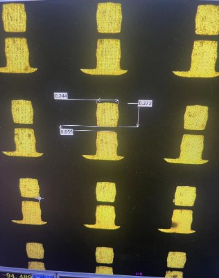
The trace width determines the amount of current a trace can carry without overheating or causing signal degradation. The clearance, on the other hand, refers to the minimum distance between traces to prevent electrical interference, short circuits, and unintended connections.
Designing with minimum trace and clearance specifications requires careful consideration of factors such as the intended application, signal integrity requirements, voltage levels, and manufacturing capabilities. Failure to adhere to these specifications can lead to various issues, including signal distortion, electrical noise, and reliability problems.
Manufacturers often provide guidelines or design rules for minimum trace and clearance requirements based on factors such as the PCB’s technology, fabrication process, and intended application. These guidelines help ensure that the final PCB meets the necessary performance and reliability standards.
What are the Minimum Trace & Clearance PCB Design Guidelines?
Minimum trace and clearance PCB design guidelines typically vary depending on the specific requirements of the project, the manufacturing process, and the capabilities of the manufacturer. However, here are some general guidelines that are commonly followed in PCB design:
- Manufacturer’s Recommendations: Always refer to the manufacturer’s design rules and specifications for minimum trace widths, clearance, and other design constraints. Different manufacturers may have slightly different capabilities and requirements.
- Signal Integrity: Ensure that traces are wide enough to carry the required current without excessive voltage drop or heating. High-speed signals may require wider traces to maintain signal integrity and reduce signal degradation.
- Voltage Considerations: Adequately space traces apart, especially when dealing with high-voltage circuits, to prevent arcing or short circuits. Pay attention to minimum clearance requirements, which are often dictated by the voltage level.
- Manufacturing Capabilities: Consider the capabilities of the PCB fabrication process, such as the minimum feature sizes and tolerances that can be reliably achieved. Design traces and spacing within the limitations of the chosen manufacturing process.
- Environmental Factors: Take into account environmental conditions such as temperature, humidity, and vibration, which may affect the performance and reliability of the PCB. Ensure that traces and clearances are designed to withstand these conditions.
- Component Placement: Optimize component placement to minimize trace lengths and reduce the need for complex routing, which can help maintain signal integrity and minimize electromagnetic interference.
- Design for Assembly (DFA): Design the PCB with ease of assembly in mind, considering factors such as component accessibility, solderability, and manufacturability. Ensure that trace routing does not impede the assembly process.
- Compliance Standards: If the PCB is intended for use in a specific industry or application, such as automotive, aerospace, or medical devices, ensure that the design complies with relevant industry standards and regulations.
- Iterative Design: PCB design is often an iterative process. Perform thorough design reviews and simulations to identify and address any potential issues early in the design phase.
By following these guidelines and best practices, designers can create PCB layouts that meet performance requirements, ensure reliability, and facilitate the manufacturing process.
Minimum Trace & Clearance PCB
What is the Minimum Trace&Clearance PCB Fabrication Process?
The PCB fabrication process involves several steps to produce a printed circuit board with minimum trace widths and clearances. Here’s an overview of the typical fabrication process:
- Design: The PCB design is created using PCB design software. This includes placing components, routing traces, and defining the minimum trace widths and clearances according to the design requirements.
- Gerber Files Generation: Once the design is finalized, Gerber files are generated. These files contain information about the PCB layers, traces, pads, and other features necessary for fabrication.
- Substrate Preparation: The fabrication process begins with preparing the substrate material, usually a laminate composed of layers of fiberglass reinforced with epoxy resin. The substrate is cleaned and prepared for the next steps.
- Copper Cladding: A thin layer of copper foil is bonded to the substrate material on both sides. This copper layer will form the conductive traces and pads on the finished PCB.
- Photoresist Application: A layer of photoresist material is applied to the copper-clad substrate. This photoresist will be used to selectively protect areas of the copper during the etching process.
- Exposure and Development: The Gerber files are used to create a photo mask, which is used to expose the photoresist to UV light. The exposed areas harden, while the unexposed areas are washed away during development, leaving behind a pattern of photoresist.
- Etching: The PCB is submerged in an etchant solution, typically containing chemicals such as ferric chloride or ammonium persulfate. The etchant dissolves the unprotected copper, leaving behind the desired conductive traces and pads defined by the photoresist pattern.
- Strip and Clean: After etching, the remaining photoresist is stripped away, leaving behind clean copper traces and pads on the substrate. The PCB is thoroughly cleaned to remove any residues from the etching process.
- Drilling: Holes are drilled in the PCB to accommodate through-hole components and vias. These holes are plated with copper to provide electrical connections between layers if necessary.
- Surface Finish: A surface finish is applied to protect the exposed copper surfaces and provide solderability. Common surface finishes include HASL (Hot Air Solder Leveling), ENIG (Electroless Nickel Immersion Gold), and OSP (Organic Solderability Preservative).
- Silkscreen Printing: Finally, component designators, logos, and other markings are printed onto the PCB using a silkscreening process for component placement guidance and identification.
- Inspection and Testing: The finished PCB undergoes inspection and testing to ensure that it meets the design specifications, including minimum trace widths and clearances. This may involve visual inspection, electrical testing, and functionality testing.
By following these steps carefully, PCB manufacturers can produce boards with minimum trace widths and clearances that meet the design requirements and ensure reliable performance in electronic devices.
How do you manufacture a Minimum Trace&Clearance PCB?
Manufacturing a Minimum Trace and Clearance PCB involves following specific processes and techniques to ensure that the desired trace widths and clearances are achieved accurately. Here’s a general overview of the steps involved:
- Design Verification: Before manufacturing, ensure that the PCB design meets the minimum trace and clearance requirements. Use PCB design software to verify that the traces and clearances adhere to the specified dimensions.
- Material Selection: Choose PCB substrate materials that meet the requirements for the desired minimum trace and clearance. High-quality laminate materials with fine copper foil thickness are typically used for manufacturing PCBs with tight tolerances.
- Photolithography: The PCB manufacturing process typically involves photolithography to define the trace patterns on the copper-clad substrate. A layer of photoresist is applied to the substrate, exposed to UV light through a photomask, and developed to create the desired pattern of traces and clearances.
- Etching: After photolithography, the PCB is immersed in an etchant solution to remove the exposed copper and define the conductive traces. The etching process must be carefully controlled to achieve the desired trace widths and maintain sufficient clearance between traces.
- Drilling: Holes are drilled in the PCB to accommodate through-hole components and vias. The drilling process must be precise to ensure that the holes are aligned accurately with the trace patterns and do not compromise the minimum clearance requirements.
- Plating: If the PCB design includes plated through-holes or vias, a plating process is used to deposit a thin layer of copper onto the hole walls. This enhances conductivity and ensures reliable electrical connections between layers while maintaining the required clearance.
- Surface Finish: Apply a surface finish to protect the exposed copper surfaces and provide solderability. Common surface finishes include HASL (Hot Air Solder Leveling), ENIG (Electroless Nickel Immersion Gold), and OSP (Organic Solderability Preservative).
- Quality Control: Throughout the manufacturing process, perform rigorous quality control checks to verify that the trace widths and clearances meet the specified dimensions. Use automated optical inspection (AOI) and other testing methods to detect any defects or deviations from the design requirements.
- Final Inspection: After manufacturing, conduct a final inspection of the finished PCB to ensure that it meets the minimum trace and clearance specifications. Inspect the PCB for any defects, irregularities, or deviations from the design.
By following these manufacturing steps carefully and employing quality control measures, manufacturers can produce Minimum Trace and Clearance PCBs that meet the required specifications and ensure reliable performance in electronic devices.
How much should a Minimum Trace&Clearance PCB cost?
The cost of manufacturing a Minimum Trace and Clearance PCB can vary significantly depending on various factors such as:
- Board Size: Larger PCBs typically cost more due to the increased material and manufacturing time required.
- Layer Count: PCBs with more layers generally cost more to manufacture due to the complexity of the fabrication process.
- Trace Width and Clearance: PCBs with tighter trace widths and clearances may require more precise manufacturing processes, which can increase costs.
- Material: The choice of substrate material and surface finish can affect the cost. High-quality materials and finishes may incur higher costs.
- Quantity: Economies of scale apply to PCB manufacturing, meaning that larger production runs generally result in lower per-unit costs.
- Lead Time: Expedited manufacturing services typically come with higher costs compared to standard lead times.
- Additional Features: Extra features such as controlled impedance, blind/buried vias, and special finishes can add to the overall cost.
- Supplier: Different PCB manufacturers have varying pricing structures, capabilities, and quality levels, which can impact the cost.
As a rough estimate, the cost of manufacturing a Minimum Trace and Clearance PCB can range from a few dollars for simple single-layer boards to hundreds or even thousands of dollars for complex multilayer boards with tight tolerances and special features. It’s recommended to obtain quotes from multiple PCB manufacturers to compare prices and find the best balance between cost, quality, and lead time for your specific requirements.
What is Minimum Trace&Clearance PCB base material?
The base material for Minimum Trace and Clearance PCBs, like most other types of PCBs, typically consists of a laminate composed of layers of substrate material and copper foil. The substrate material provides mechanical support and insulation between the conductive layers, while the copper foil forms the conductive traces and pads.
The choice of base material depends on various factors, including the desired electrical performance, thermal properties, cost considerations, and manufacturability. Common base materials used for Minimum Trace and Clearance PCBs include:
- FR-4: FR-4 (Flame Retardant 4) is the most widely used substrate material for PCBs. It is a glass-reinforced epoxy laminate known for its good electrical insulation properties, mechanical strength, and affordability. FR-4 is suitable for a wide range of applications and can meet minimum trace and clearance requirements with proper design and manufacturing techniques.
- High-Speed Materials: For applications requiring high-frequency signals or stringent impedance control, specialized high-speed materials such as FR-4 with high-speed additives, Rogers laminates, or other advanced materials may be used. These materials offer superior electrical performance but may come at a higher cost.
- Flex and Rigid-Flex Materials: Flex and rigid-flex PCBs, which allow for bending or folding, use flexible substrate materials such as polyimide (PI) or polyester (PET) in addition to rigid materials like FR-4. These materials can meet minimum trace and clearance requirements while offering flexibility for applications with space constraints or complex form factors.
- Metal Core Materials: Metal core PCBs use a metal substrate, typically aluminum or copper, for enhanced thermal conductivity and heat dissipation. They are commonly used in high-power applications or LED lighting where heat management is crucial.
- Ceramic Materials: Ceramic substrates offer excellent thermal properties and stability at high temperatures, making them suitable for demanding applications such as power electronics or RF/microwave circuits.
Ultimately, the choice of base material for Minimum Trace and Clearance PCBs depends on the specific requirements of the application, including electrical performance, thermal management, mechanical properties, and cost considerations. It’s essential to select a material that meets the necessary specifications while ensuring reliability and manufacturability.
Which company makes Minimum Trace&Clearance PCB?
There are many companies that can produce Minimum Trace and Clearance PCBs, some of which are well-known PCB manufacturers such as Mouser Electronics in the United States, Hitachi Chemical Electronics in Japan, and Lite-On Precision Electronics in Taiwan. These companies have advanced manufacturing equipment and technologies to meet various PCB design requirements, including Minimum Trace and Clearance.
As a professional PCB manufacturing company, our company is also capable of producing Minimum Trace and Clearance PCBs. We have advanced production equipment and a skilled technical team to precisely control the PCB manufacturing process to ensure meeting the customer’s requirements and standards. We strictly adhere to industry standards and quality management systems to ensure that each PCB has high quality, stability, and reliability.
Our company is committed to providing customized PCB solutions for customers, including Minimum Trace and Clearance PCBs. We can develop production plans based on customer design requirements and specifications, and provide professional technical support and advice to ensure the production of PCB products that meet customer expectations.
Whether in the fields of consumer electronics, communication equipment, medical devices, or industrial control, our company has rich experience and expertise to meet the needs of customers in different industries. We have earned the trust and praise of customers with high-quality products and services and will continue to strive to provide better service to customers.
What are the 7 qualities of good customer service?
Good customer service is essential for building positive relationships with customers and ensuring satisfaction with products or services. Here are seven qualities of good customer service:
- Responsiveness: Customers appreciate prompt responses to their inquiries, whether through phone, email, chat, or in-person interactions. Being responsive demonstrates that you value their time and concerns.
- Empathy: Empathizing with customers by understanding their needs, concerns, and emotions fosters trust and rapport. It’s crucial to listen actively and show genuine empathy when addressing their issues or requests.
- Clear Communication: Clear and effective communication is key to providing excellent customer service. Ensure that information is conveyed accurately, concisely, and in a manner that is easily understood by the customer.
- Problem-Solving Skills: Being able to identify and resolve customer issues efficiently demonstrates competence and dedication to customer satisfaction. Develop problem-solving skills to address challenges and find solutions that meet the customer’s needs.
- Professionalism: Maintaining a professional demeanor in all interactions with customers reflects positively on your company’s image and credibility. Treat customers with respect, courtesy, and professionalism at all times.
- Product Knowledge: Having a thorough understanding of the products or services you offer enables you to provide accurate information and guidance to customers. Ensure that customer service representatives are well-trained and knowledgeable about the offerings.
- Follow-up and Follow-through: Following up with customers after resolving their issues or fulfilling their requests shows that you value their feedback and satisfaction. Additionally, following through on promises or commitments reinforces trust and reliability.
By embodying these qualities, businesses can deliver exceptional customer service experiences that build loyalty, enhance brand reputation, and drive long-term success.
FAQs
What are Minimum Trace and Clearance PCBs?
Minimum Trace and Clearance PCBs refer to printed circuit boards where the conductive traces have the smallest allowable width, and there is the minimum separation distance between them. These specifications are crucial for ensuring functionality, reliability, and manufacturability.
Why are Minimum Trace and Clearance specifications important?
Minimum Trace and Clearance specifications are important because they determine the electrical performance, signal integrity, and reliability of the PCB. Adhering to these specifications helps prevent issues such as signal distortion, electrical interference, and short circuits.
What factors influence Minimum Trace and Clearance requirements?
Factors influencing Minimum Trace and Clearance requirements include the application’s voltage levels, signal frequencies, thermal considerations, manufacturing capabilities, and compliance standards.
How do I determine the Minimum Trace and Clearance for my PCB design?
The Minimum Trace and Clearance for a PCB design are typically determined based on factors such as the voltage rating of the components, signal integrity requirements, and manufacturing capabilities. PCB design software often includes design rule checks (DRC) to help ensure compliance with these specifications.
Can I reduce Minimum Trace and Clearance to save space on the PCB?
While it may be tempting to reduce Minimum Trace and Clearance to save space, doing so can lead to electrical issues such as signal degradation, crosstalk, and short circuits. It’s essential to adhere to the recommended specifications to ensure the PCB’s reliability and performance.
What manufacturing processes are used for Minimum Trace and Clearance PCBs?
Manufacturing processes for Minimum Trace and Clearance PCBs include photolithography, etching, drilling, plating, surface finishing, and inspection. These processes require precision and control to achieve the desired trace widths and clearances.
Are there specific design guidelines for Minimum Trace and Clearance PCBs?
Yes, there are specific design guidelines for Minimum Trace and Clearance PCBs provided by PCB manufacturers and industry standards organizations. These guidelines help ensure that the PCB design meets the necessary performance and reliability standards.
Can I use off-the-shelf components with Minimum Trace and Clearance PCBs?
Yes, off-the-shelf components can typically be used with Minimum Trace and Clearance PCBs as long as the PCB design accommodates the component footprint and follows proper design practices for assembly and soldering.