
Multilayer Ceramic Substrate Manufacturer
Multilayer Ceramic Substrate Manufacturer,Multilayer Ceramic Substrates are high-performance electronic components constructed from multiple layers of ceramic materials, typically alumina or ceramic composites. These substrates offer exceptional electrical insulation and thermal conductivity, making them ideal for applications requiring robust performance under high-frequency or high-power conditions. The multilayer design allows for complex circuitry and high-density interconnections, supporting advanced electronic functions in compact spaces. These substrates are widely used in telecommunications, automotive electronics, and power management systems due to their durability, reliability, and superior thermal management. Their ability to handle demanding electrical and thermal requirements makes them essential in modern electronic devices.
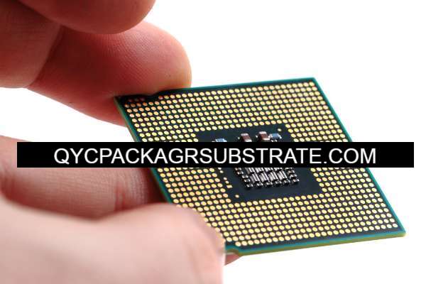
What is a Multilayer Ceramic Substrate?
A multilayer ceramic substrate is an advanced electronic packaging material made using a multilayer ceramic lamination technique, which integrates multiple circuits and components onto a single substrate. This substrate is primarily composed of high-performance ceramic materials such as alumina, aluminum nitride, or silicon nitride. Through high-temperature or low-temperature co-firing techniques, multiple ceramic layers and conductive paths (such as metalized vias and traces) are integrated together.
Multilayer ceramic substrates offer excellent electrical, thermal, and mechanical properties, making them widely used in high-performance and high-reliability applications. Their high thermal conductivity allows effective heat dissipation, making them suitable for high-power electronic devices and circuits. Additionally, ceramic materials provide good insulation and stability, maintaining consistent electrical characteristics under harsh environmental conditions. The multilayer structure also enables complex circuit designs within limited space, enhancing circuit integration and miniaturization.
These substrates are used extensively in various high-end applications, including aerospace, military, automotive electronics, telecommunications, and high-frequency communication devices. The application scope has also expanded to microelectronics packaging, such as multi-chip modules (MCMs) and system-in-package (SiP), where compact size, lightweight, and high reliability are crucial.
With technological advancements, the manufacturing techniques and materials for multilayer ceramic substrates continue to innovate and improve. For example, the development of low-temperature co-fired ceramics (LTCC) and high-temperature co-fired ceramics (HTCC) has made the manufacturing process more flexible and efficient, further enhancing the application potential of multilayer ceramic substrates in modern electronic packaging.
In summary, multilayer ceramic substrates, with their outstanding performance and broad application prospects, have become an essential material in the field of electronic packaging, driving the development of electronic products towards higher performance and miniaturization.
Multilayer Ceramic Substrate Manufacturer
What are the Multilayer Ceramic Substrate Design Guidelines?
Multilayer ceramic substrate design guidelines are crucial for ensuring the optimal performance, reliability, and manufacturability of ceramic substrates in electronic applications. Here are key considerations and best practices for designing multilayer ceramic substrates:
- Material Selection: Choose appropriate ceramic materials based on the specific application requirements. Common materials include alumina (Al₂O₃), aluminum nitride (AlN), and silicon nitride (Si₃N₄). Consider factors such as thermal conductivity, dielectric constant, and mechanical strength.
- Layer Structure: Design the layer stack-up carefully, taking into account the required number of layers and their functions. Ensure proper alignment and registration of each layer to avoid defects during manufacturing.
- Circuit Design:Plan the layout of the conductive paths, vias, and pads to minimize interference and signal loss. Use appropriate trace widths and spacing to handle the expected current and prevent signal degradation.
- Thermal Management: Incorporate thermal vias and heat spreaders to manage heat dissipation effectively. Consider the thermal expansion coefficients of the ceramic and the components to avoid thermal stress and potential damage.
- Mechanical Design: Ensure the mechanical integrity of the substrate by considering factors such as the stress and strain on the ceramic during manufacturing and operation. Design for sufficient support and reinforcement to prevent cracking or warping.
- Manufacturing Constraints: Be aware of the limitations of the manufacturing processes, such as co-firing temperatures and tolerances. Design with these constraints in mind to ensure that the substrate can be produced reliably and cost-effectively.
- Electrical Performance: Optimize the substrate design for electrical performance, including signal integrity and impedance matching. Use simulation tools to predict and improve the electrical behavior of the substrate.
- Testing and Validation: Plan for comprehensive testing and validation of the substrate design to ensure it meets all performance and reliability requirements. This includes electrical testing, thermal cycling, and mechanical stress tests.
- Cost Considerations: Balance design complexity with cost constraints. While advanced features and high performance can increase costs, ensure that the design remains within budget and offers a good return on investment.
- Compliance and Standards: Adhere to industry standards and guidelines relevant to ceramic substrates, such as those from IPC (Institute for Printed Circuits) and other relevant organizations, to ensure compatibility and quality.
By following these guidelines, designers can create high-performance multilayer ceramic substrates that meet the needs of modern electronic systems and applications, ensuring reliability and efficiency throughout their lifecycle.
What is the Multilayer Ceramic Substrate Fabrication Process?
The fabrication process for multilayer ceramic substrates involves several key steps, each critical for achieving the desired electrical, thermal, and mechanical properties. Here is an overview of the typical fabrication process:
- Material Preparation: The process begins with the preparation of ceramic powders, which are mixed with binders and additives to form a slurry. This slurry is then used to produce green sheets through processes like tape casting or screen printing. The choice of ceramic material—such as alumina, aluminum nitride, or silicon nitride—depends on the application requirements.
- Green Sheet Formation: The ceramic slurry is cast into thin, flat sheets, known as green sheets. These sheets are dried to remove excess solvents, resulting in a flexible but fragile material that can be handled and stacked.
- Layer Stacking:Multiple green sheets are stacked to form the desired number of layers for the substrate. Between the layers, conductive patterns and vias are added using screen printing or photolithography techniques. These patterns are created using metal pastes or inks that will later be fired to form the conductive traces.
- Lamination: The stacked layers are then laminated together under heat and pressure. This step consolidates the layers and ensures strong adhesion between them. The lamination process must be carefully controlled to prevent delamination or warping.
- Co-Firing: After lamination, the substrate undergoes co-firing, where it is heated in a kiln to high temperatures. During this process, the organic binders are burned off, and the ceramic material is sintered to form a solid, dense substrate. This step also converts the metal patterns into conductive traces.
- Via Drilling: Once co-firing is complete, vias (holes) are drilled or laser-cut into the substrate. These vias provide electrical connections between different layers of the substrate.
- Plating and Metallization: The drilled vias and surface areas are then plated with metal, typically copper, to create electrical connections. This step often involves electroplating or sputtering techniques to deposit a thin layer of metal.
- Patterning and Etching: The metal layers are patterned using photolithography and etching processes to define the final circuitry. This step involves applying a photoresist layer, exposing it to light through a mask, and etching away the unwanted metal to leave behind the desired circuit patterns.
- Inspection and Testing: The fabricated substrates undergo rigorous inspection and testing to ensure they meet the required specifications. This includes checking for defects, verifying electrical performance, and ensuring dimensional accuracy.
- Final Processing: Any additional processes, such as surface finishing or application of protective coatings, are performed as needed. The substrates are then cleaned and prepared for assembly with electronic components.
Each step in the fabrication process is critical for achieving the high performance and reliability required in multilayer ceramic substrates. The precision and quality control throughout the process ensure that the final product meets the stringent demands of modern electronic applications.
How Do You Manufacture a Multilayer Ceramic Substrate?
Manufacturing a multilayer ceramic substrate involves a series of carefully controlled steps to produce a high-quality, reliable product. Here’s a detailed overview of the manufacturing process:
- Material Preparation: Start with the selection and preparation of ceramic powders, such as alumina (Al₂O₃), aluminum nitride (AlN), or silicon nitride (Si₃N₄). These powders are mixed with binders, plasticizers, and solvents to create a slurry or paste. The mixture is then homogenized to ensure uniformity.
- Green Sheet Production: The prepared slurry is cast into thin sheets, called green sheets, using techniques like tape casting or screen printing. The green sheets are then dried to remove excess solvents, resulting in a flexible yet fragile material that can be handled and layered.
- Layer Stacking: Multiple green sheets are stacked to create the desired number of layers for the substrate. Each layer includes the necessary patterns for conductive traces and vias. Conductive patterns are typically applied using screen printing or photolithography, employing metal pastes or inks that will become the electrical traces after firing.
- Lamination:The stacked green sheets are subjected to heat and pressure in a lamination press. This step consolidates the layers, bonding them together and forming a unified structure. Careful control of temperature and pressure is crucial to avoid delamination and ensure a strong bond between layers.
- Co-Firing:The laminated stack is then fired in a kiln at high temperatures, a process known as co-firing. During this phase, organic binders are burned off, and the ceramic material undergoes sintering to form a solid, dense substrate. Metal traces in the vias are also sintered to create reliable electrical connections.
- Via Drilling: After co-firing, vias (holes) are drilled or laser-cut into the substrate to provide vertical electrical connections between layers. Precision in drilling is essential to ensure correct alignment and functionality.
- Plating and Metallization: The vias and exposed surface areas are plated with metal, often copper, to establish electrical connectivity. This process involves techniques like electroplating or sputtering to deposit a thin, uniform layer of metal.
- Patterning and Etching: The metal layers are then patterned to define the final circuit layout. This involves applying a photoresist layer, exposing it to UV light through a mask, and etching away the unwanted metal to leave the desired circuit pattern.
- Inspection and Testing: The substrates undergo rigorous quality control measures, including visual inspection, electrical testing, and dimensional verification. This ensures that the substrates meet performance specifications and are free from defects.
- Final Processing: Any additional finishing processes, such as applying protective coatings or surface treatments, are carried out. The substrates are cleaned and prepared for the final assembly with electronic components.
Each stage of the manufacturing process is critical to producing high-quality multilayer ceramic substrates. Precision and control throughout the process ensure that the final product meets the demanding requirements of modern electronic applications.
How Much Should a Multilayer Ceramic Substrate Cost?
The cost of a multilayer ceramic substrate can vary significantly based on several factors, including material type, complexity, size, and volume. Here’s a breakdown of the key factors influencing the cost:
- Material Type: The choice of ceramic material affects the cost. Common materials include alumina, aluminum nitride, and silicon nitride, each with different price points based on their properties and processing requirements. High-performance materials or those with specialized properties typically cost more.
- Complexity and Design: The complexity of the substrate design impacts cost. More layers, intricate circuitry, and additional features such as embedded components or high-density interconnects (HDI) can increase manufacturing costs. Custom designs with unique specifications or tight tolerances will generally be more expensive.
- Size and Dimensions: Larger substrates or those with larger surface areas require more material and can increase production costs. The size of the substrate also influences the cost of equipment and processing.
- Volume and Quantity: Economies of scale play a significant role in the cost of multilayer ceramic substrates. Higher production volumes generally lead to lower per-unit costs due to shared setup and manufacturing expenses. Conversely, low-volume or prototype runs may be more costly per unit.
- Manufacturing Process:The choice of manufacturing processes and technology affects cost. Processes like high-temperature co-firing, precision drilling, and advanced patterning techniques can add to the cost. Additionally, specialized processes for achieving high performance or reliability can further increase costs.
- Quality and Reliability Requirements: Substrates designed for high-reliability applications, such as aerospace or medical devices, may incur additional costs due to stringent quality control, testing, and certification requirements.
- Additional Features: Any additional features, such as custom metallization, surface treatments, or embedded components, can add to the cost. Advanced features require more complex processing and quality control.
- Supplier and Market Conditions: The cost can also be influenced by the supplier’s pricing structure, market demand, and regional factors. Prices may vary based on the supplier’s capabilities, geographic location, and current market trends.
For precise cost estimates, it is advisable to consult with manufacturers and suppliers, provide detailed specifications, and request quotes based on specific project requirements. This ensures an accurate understanding of the costs involved and helps in budgeting for production.
What is the Base Material for a Multilayer Ceramic Substrate?
The base material for a multilayer ceramic substrate is typically a type of high-performance ceramic that provides the necessary electrical, thermal, and mechanical properties required for advanced electronic applications. Here’s an overview of the most common base materials used:
- Alumina (Al₂O₃): Alumina, also known as aluminum oxide, is the most widely used ceramic material for multilayer substrates. It offers good electrical insulation, thermal conductivity, and mechanical strength. Alumina is relatively inexpensive and suitable for a broad range of applications, including general electronics and some high-frequency applications.
- Aluminum Nitride (AlN):Aluminum nitride is known for its excellent thermal conductivity, making it ideal for applications requiring efficient heat dissipation. It also has good electrical insulation properties. Due to its high thermal conductivity, it is often used in high-power and high-performance electronic devices.
- Silicon Nitride (Si₃N₄): Silicon nitride provides superior mechanical strength, thermal shock resistance, and thermal conductivity. It is used in applications where high durability and resistance to thermal cycling are required. It is typically more expensive than alumina but offers enhanced performance in demanding environments.
- Beryllium Oxide (BeO): Beryllium oxide is used in specialized applications due to its high thermal conductivity and electrical insulation properties. However, due to its toxicity and high cost, it is less commonly used compared to other materials. It is primarily used in high-power and high-frequency applications where its unique properties are required.
- Cordierite: Cordierite is a ceramic material known for its thermal shock resistance and low thermal expansion. It is used in applications where temperature fluctuations are a concern. It is not as commonly used as alumina or aluminum nitride but can be valuable in specific applications requiring thermal stability.
- LTCC (Low-Temperature Co-Fired Ceramic): LTCC materials are a type of ceramic used in the manufacture of multilayer substrates that can be co-fired at lower temperatures. This material allows for the integration of additional components and circuitry within the substrate. LTCC is often used in applications requiring complex, multi-layered circuit designs.
- HTCC (High-Temperature Co-Fired Ceramic): HTCC materials are used for substrates that need to be fired at higher temperatures. They provide high mechanical strength and are used in applications that require robust substrates capable of withstanding high thermal stresses.
Each of these materials has specific advantages and applications, and the choice of base material depends on the requirements of the intended application, including thermal management, electrical performance, and mechanical durability.
Which Company Makes Multilayer Ceramic Substrates?
Many companies around the world manufacture multilayer ceramic substrates, playing crucial roles in high-performance electronic packaging and advanced applications. Here are some notable manufacturers and their features:
- Murata Manufacturing Co., Ltd.: As a global leader in electronic components, Murata offers a wide range of multilayer ceramic substrate products, covering various needs from general electronics to high-frequency and high-power applications. Their products are known for high quality and reliability.
- Kyocera Corporation: Kyocera has extensive experience in ceramic materials and electronic components, providing high-performance multilayer ceramic substrates suitable for communication, automotive electronics, and industrial applications. Their products are renowned for high thermal conductivity and excellent mechanical strength.
- Taiyo Yuden Co., Ltd.: Taiyo Yuden focuses on producing various electronic components, including multilayer ceramic substrates. Their products are widely used in consumer electronics and communication devices, recognized for their innovative designs and reliable performance.
- NGK Insulators, Ltd.: NGK Insulators has a long history in ceramic substrates, offering multilayer ceramic substrates for high-end applications such as automotive and energy sectors. Their substrates are known for exceptional thermal management performance and high reliability.
- Samsung Electro-Mechanics Co., Ltd.: Samsung Electro-Mechanics manufactures multilayer ceramic substrates primarily used in mobile devices and consumer electronics. Their products meet modern electronic product demands with high integration and performance.
- Yageo Corporation: Yageo produces various electronic components, including multilayer ceramic substrates, for automotive, industrial, and consumer electronics applications. They are dedicated to providing high-quality and cost-effective products.
Our company also specializes in manufacturing multilayer ceramic substrates and offers professional production services. Our multilayer ceramic substrates feature the following characteristics:
– High-Performance Materials: We use high-quality ceramic materials such as alumina, aluminum nitride, and silicon nitride to ensure excellent electrical insulation, thermal management, and mechanical strength.
– Advanced Manufacturing Processes: We employ advanced lamination, co-firing, and metallization processes to ensure high quality and consistency in every substrate. Our manufacturing process is strictly controlled to meet high performance and reliability requirements.
– Custom Solutions: We provide customized multilayer ceramic substrate solutions based on specific customer needs. Whether it’s complex circuit designs or specific size requirements, we deliver products that meet customer specifications.
– Comprehensive Testing: We perform comprehensive testing and inspection on every batch of products during production to ensure they meet industry standards and customer requirements.
– Customer Support: We offer professional technical support and after-sales service, ensuring customers receive full assistance throughout the design, manufacturing, and usage phases.
Through our high-quality multilayer ceramic substrates and excellent service, we are committed to meeting the needs of various high-end electronic applications and providing reliable solutions for our customers.
What are the 7 Qualities of Good Customer Service?
Good customer service is essential for building strong relationships with clients and ensuring their satisfaction. Here are seven key qualities that define excellent customer service:
- Responsiveness:Quick and efficient responses to customer inquiries and issues are crucial. Customers appreciate timely answers to their questions and swift resolutions to their problems. Responsiveness shows that the company values the customer’s time and is dedicated to providing effective support.
- Empathy:Understanding and empathizing with customers’ concerns and frustrations is vital. Empathy involves actively listening to customers, acknowledging their feelings, and providing support that addresses their emotional and practical needs. This helps build a connection and fosters trust.
- Knowledgeability: A strong understanding of the company’s products or services, as well as relevant policies and procedures, is essential. Customer service representatives should be well-trained and knowledgeable, enabling them to provide accurate information, solve problems effectively, and offer relevant advice.
- Communication Skills: Clear and effective communication is fundamental to good customer service. Representatives should be able to convey information in a straightforward, polite, and professional manner. This includes active listening, clear articulation of solutions, and avoiding jargon that might confuse the customer.
- Patience: Patience is important when dealing with customers, especially when they are frustrated or confused. Customer service representatives should remain calm and composed, taking the time to thoroughly address concerns and provide detailed explanations as needed.
- Personalization:Tailoring interactions to meet the specific needs and preferences of individual customers enhances their experience. Personalized service involves remembering past interactions, addressing customers by name, and providing solutions that are relevant to their unique situation.
- Follow-Up: Good customer service involves checking back with customers to ensure that their issues have been resolved to their satisfaction. Follow-up demonstrates a commitment to quality service and helps prevent future problems by addressing any lingering concerns.
Incorporating these qualities into customer service practices can significantly enhance customer satisfaction, build loyalty, and contribute to a positive reputation for the company.
FAQs about Multilayer Ceramic Substrates
What is a multilayer ceramic substrate?
A multilayer ceramic substrate is a type of electronic component made by stacking and laminating multiple layers of ceramic material, each with conductive patterns, to create a compact and high-performance substrate used for electronic circuits and components.
What materials are used in multilayer ceramic substrates?
Common materials include alumina (Al₂O₃), aluminum nitride (AlN), and silicon nitride (Si₃N₄). These materials are chosen based on their electrical insulation, thermal conductivity, and mechanical strength properties.
What are the main advantages of using multilayer ceramic substrates?
Advantages include high thermal conductivity, excellent electrical insulation, compact design, and the ability to integrate multiple layers of circuitry and components in a single substrate. They are suitable for high-frequency and high-power applications.
What applications use multilayer ceramic substrates?
They are used in various applications such as telecommunications, automotive electronics, medical devices, and consumer electronics. They are especially useful in high-power and high-frequency circuits where thermal management and electrical performance are critical.
How are multilayer ceramic substrates manufactured?
The manufacturing process typically involves creating green ceramic sheets, stacking and laminating them, co-firing to sinter the ceramic and metal patterns, drilling vias, and then plating and patterning the metal layers.
What factors affect the cost of multilayer ceramic substrates?
Cost factors include material type, substrate complexity, size, production volume, and manufacturing processes. Custom designs and high-performance materials generally increase the cost.
Can multilayer ceramic substrates be customized?
Yes, they can be customized to meet specific design requirements, including size, layer count, circuit patterns, and material properties. Customization allows for tailored solutions to fit particular applications.