
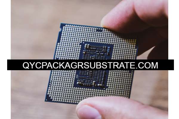
MW4000 Materials PCB Manufacturer
MW4000 Materials PCB Manufacturer,MW4000 Materials PCB is a high-performance printed circuit board material designed specifically for microwave (MW) and high-frequency (HF) applications. This material exhibits excellent dielectric properties and low loss characteristics, typically based on PTFE (polytetrafluoroethylene) substrate, effectively minimizing signal attenuation and crosstalk. MW4000 Materials PCBs are intricately designed with controlled impedance traces, optimized ground planes, and shielding techniques to ensure reliability and stability in microwave frequency bands. They are widely used in communication systems, radar, satellite communications, and high-speed data transmission, providing crucial performance support and reliability assurance for modern electronic devices.
What is MW4000 Materials PCB?
The MW4000 Materials PCB refers to a type of printed circuit board (PCB) designed specifically to meet stringent requirements in terms of material properties, reliability, and performance. Typically, PCBs are constructed using various materials such as fiberglass epoxy laminates (FR-4), but advanced applications, like those requiring high-frequency signals or demanding environments, may necessitate specialized materials.
The “MW4000” designation likely indicates a specific material grade or series developed by a manufacturer. These materials are engineered to offer characteristics such as low dielectric constant, low loss tangent, excellent thermal stability, and possibly enhanced mechanical properties. They are crucial in applications where signal integrity, durability under harsh conditions, or high-speed data transmission are critical factors.
PCBs using MW4000 materials are often found in telecommunications equipment, aerospace technology, radar systems, and other high-performance electronic devices. Their ability to maintain signal integrity at higher frequencies and withstand environmental stresses makes them ideal for demanding industrial and commercial applications.
In summary, MW4000 Materials PCBs represent an advanced category of printed circuit boards tailored to meet the exacting requirements of modern electronic and communication systems, offering superior performance and reliability compared to standard PCB materials.
MW4000 Materials PCB Manufacturer
What are MW4000 Materials PCB Design Guidelines?
Design guidelines for MW4000 Materials PCB focus on ensuring optimal performance and reliability in high-frequency and demanding applications. Here are some key considerations:
- Material Selection: Choose MW4000 series materials that best suit the specific application requirements, considering factors such as dielectric constant (εr), loss tangent (tanδ), thermal conductivity, and mechanical properties.
- Layer Stackup: Design an appropriate layer stackup to minimize signal losses and interference. Use controlled impedance traces to maintain signal integrity, especially for high-frequency signals.
- Trace Routing: Implement differential pair routing for critical signals to minimize crosstalk and maintain impedance control. Maintain adequate spacing between traces and ground planes to reduce electromagnetic interference (EMI).
- Via Design: Optimize via structures to minimize signal reflections and impedance variations. Consider using via stub removal techniques or backdrilling for high-frequency applications.
- Grounding: Ensure a solid ground plane beneath signal layers to provide a low-impedance return path for signals and to shield against external noise. Use multiple vias for ground connections to reduce ground bounce.
- Component Placement: Place critical components strategically to minimize trace lengths and reduce parasitic capacitance and inductance. Follow best practices for signal routing around sensitive components.
- Thermal Management: Consider thermal dissipation requirements and ensure adequate thermal vias and heat sinking for components that generate heat. MW4000 materials often have good thermal conductivity, but thermal management is still crucial in high-power applications.
- Manufacturability: Design with manufacturability in mind, considering the capabilities of PCB fabrication and assembly processes compatible with MW4000 materials. Ensure that design rules are followed to avoid fabrication issues.
- Testing and Validation: Plan for testing and validation of the PCB design to ensure it meets performance specifications. Consider high-frequency testing techniques to verify signal integrity and impedance matching.
- Environmental Considerations: MW4000 materials may have specific environmental considerations such as temperature stability and resistance to moisture. Ensure the design can withstand the intended operating conditions.
By adhering to these design guidelines, engineers can maximize the performance and reliability of MW4000 Materials PCBs in applications requiring high-frequency operation, low signal loss, and robustness against environmental factors.
What is the MW4000 Materials PCB Fabrication Process?
The fabrication process for MW4000 Materials PCBs involves several specialized steps to ensure the desired material properties and performance characteristics are achieved. Here’s an overview of the typical fabrication process:
- Material Selection: Choose the appropriate MW4000 series material based on the specific application requirements. MW4000 materials are selected for their high-frequency performance, low dielectric loss, thermal stability, and mechanical strength.
- Preparation of Substrates: Start with preparing the substrate materials. MW4000 materials may come in laminate form, which is typically composed of layers of glass fabric impregnated with epoxy resin or other composite materials.
- Layer Stackup Design: Design the layer stackup according to the PCB specifications. This includes determining the number of layers, copper thickness, and the arrangement of signal and ground planes. Special attention is paid to maintaining controlled impedance for high-speed signals.
- Copper Cladding: Apply copper foil to both sides of the substrate material through a lamination process. This involves cleaning the substrate surface, applying an adhesive layer, and then laminating the copper foil under heat and pressure.
- Etching: Use chemical etching or milling processes to remove excess copper from the substrate, leaving behind the desired circuit traces and pads as per the PCB design.
- Drilling: Drill holes (vias) at specified locations to connect different layers of the PCB. For MW4000 materials, special attention is given to via placement and design to minimize signal degradation and impedance variations.
- Via Plating:Electroplate the vias with copper to ensure electrical connectivity between different layers of the PCB. This process enhances reliability and signal integrity by reducing resistance and providing a robust electrical connection.
- Surface Finish: Apply a surface finish to protect the exposed copper circuitry from oxidation and ensure solderability during assembly. Common surface finishes include HASL (Hot Air Solder Leveling), ENIG (Electroless Nickel Immersion Gold), and OSP (Organic Solderability Preservatives).
- Solder Mask Application: Apply solder mask over the PCB surface except where contacts and pads are exposed. The solder mask protects the copper traces from environmental factors and prevents unintended solder bridges during assembly.
- Silkscreen Printing: Optionally, add silkscreen legends and markings on the PCB surface to indicate component placement, polarity, and other relevant information.
- Testing and Inspection: Perform electrical testing, such as continuity checks, insulation resistance tests, and possibly high-frequency testing to ensure the PCB meets design specifications for impedance, signal integrity, and reliability.
- Quality Control:Conduct final inspection to verify dimensional accuracy, adherence to design specifications, and overall quality before the PCBs are packaged and shipped.
The fabrication of MW4000 Materials PCBs involves precision manufacturing techniques to ensure high reliability and performance, particularly in applications requiring high-frequency operation and stringent electrical characteristics. Each step in the process is crucial to achieving a PCB that meets the demanding requirements of modern electronic and communication systems.
How do you manufacture MW4000 Materials PCB?
Manufacturing MW4000 Materials PCBs involves a series of specialized steps tailored to harness the material’s properties for high-performance applications. Here’s a structured outline of the manufacturing process:
- Material Selection: Choose MW4000 series materials based on application requirements, considering factors like dielectric constant, loss tangent, thermal stability, and mechanical strength.
- Preparation of Substrates: Prepare MW4000 laminate sheets by stacking layers of glass fabric impregnated with epoxy resin or other composite materials. Ensure cleanliness and uniformity of the substrate surfaces.
- Layer Stackup Design: Design the PCB’s layer stackup according to specifications, determining the number of layers, thickness of copper foils, and placement of signal and ground planes. Consider controlled impedance requirements for high-frequency signals.
- Copper Foil Lamination:Apply copper foil to both sides of the substrate through a lamination process. This involves cleaning, applying adhesive, and then laminating the copper foil under heat and pressure to ensure strong adhesion.
- Etching: Use chemical etching or milling techniques to remove excess copper from the substrate, leaving behind the desired circuit patterns as per the PCB design. This process defines the traces, pads, and other conductive features.
- Drilling: Drill holes (vias) at designated locations to establish electrical connections between different layers of the PCB. Precision drilling techniques are crucial to ensure alignment and reliability in high-frequency applications.
- Via Plating: Electroplate the vias with copper to enhance conductivity and ensure reliable electrical connections between layers. This step involves depositing a conductive material inside the drilled holes to maintain signal integrity.
- Surface Finishing: Apply a suitable surface finish to protect exposed copper surfaces from oxidation and facilitate soldering during component assembly. Common finishes include HASL, ENIG, and OSP, chosen based on environmental and assembly requirements.
- Solder Mask Application: Apply solder mask over the PCB surface, leaving openings only where soldering is required for components. Solder mask protects copper traces from environmental factors and prevents solder bridges during assembly.
- Silkscreen Printing: Optionally, print silkscreen legends and markings on the PCB surface to indicate component placement, polarity, and other necessary information. This aids in assembly and troubleshooting.
- Electrical Testing: Perform rigorous electrical tests to verify the integrity and functionality of the PCB. Tests may include continuity checks, insulation resistance measurement, and high-frequency testing to ensure adherence to design specifications.
- Final Inspection and Quality Control: Conduct comprehensive inspection to verify dimensional accuracy, alignment of features, and overall quality of finished PCBs. Ensure compliance with industry standards and customer requirements before packaging and shipment.
Manufacturing MW4000 Materials PCBs demands precise execution at each stage to leverage the material’s properties effectively for applications requiring high-frequency performance, reliability, and robustness in diverse environmental conditions. Following these steps ensures the production of PCBs that meet stringent performance standards essential in modern electronics and communication systems.
How much should MW4000 Materials PCB cost?
The cost of MW4000 Materials PCBs can vary widely depending on several factors, including the following:
- Material Cost: MW4000 series materials are typically more expensive than standard FR-4 or other common PCB materials due to their advanced properties such as high-frequency performance, low dielectric loss, and thermal stability.
- Complexity of Design: The complexity of the PCB design influences the cost. More intricate designs with dense trace routing, multiple layers, and controlled impedance requirements may incur higher fabrication costs.
- Layer Count: PCBs with more layers generally cost more to manufacture due to increased material and processing requirements.
- Surface Finish and Additional Features: The choice of surface finish (e.g., HASL, ENIG, OSP) and additional features like silkscreen printing, special via types (e.g., blind vias, buried vias), and edge plating can impact the overall cost.
- Quantity:Economies of scale apply in PCB manufacturing. Larger quantities typically reduce the cost per unit due to efficiencies in production and setup.
- Manufacturer and Location: PCB manufacturing costs can vary depending on the capabilities and location of the manufacturer. Different regions may have different labor costs, overheads, and material availability, influencing pricing.
- Lead Time: Urgency in delivery may incur expedited manufacturing costs or impact pricing negotiations.
To provide a general estimate, MW4000 Materials PCBs could range from several dollars to tens or even hundreds of dollars per square foot, depending on the aforementioned factors. For a more precise cost estimate, it’s advisable to consult with PCB manufacturers who specialize in high-frequency and advanced material PCBs. They can provide detailed quotes based on specific design requirements and production volumes.
What is MW4000 Materials PCB base material?
MW4000 Materials PCB typically refers to a category of advanced base materials used in printed circuit board (PCB) manufacturing. The exact composition and formulation of MW4000 materials can vary depending on the specific manufacturer and product line. However, in general terms, MW4000 Materials PCB base material is characterized by the following key properties:
- Substrate Material: MW4000 materials are often based on specialized laminate substrates composed of layers of fiberglass (glass cloth) impregnated with epoxy resin or other high-performance thermosetting resin systems. These substrates provide mechanical stability, dimensional accuracy, and dielectric properties suitable for high-frequency applications.
- Dielectric Constant (εr): MW4000 materials are engineered to have a low dielectric constant, which is crucial for maintaining signal integrity and reducing signal loss, especially at higher frequencies.
- Loss Tangent (tanδ): They typically exhibit a low loss tangent, indicating minimal energy dissipation as signals propagate through the PCB. This property is essential for applications requiring high-speed data transmission and low noise performance.
- Thermal Properties: MW4000 materials often possess good thermal stability and can withstand higher temperatures compared to standard FR-4 materials. This thermal resilience is beneficial for applications where PCBs may be exposed to elevated operating temperatures.
- Mechanical Strength: The base materials used in MW4000 PCBs offer robust mechanical properties, including high tensile strength and dimensional stability, which are critical for maintaining reliability and durability in various environmental conditions.
- Manufacturability: MW4000 materials are designed to be compatible with standard PCB manufacturing processes such as lamination, etching, drilling, and surface finishing. They allow for precise fabrication of intricate PCB designs while maintaining material integrity and performance characteristics.
Overall, MW4000 Materials PCB base material represents an advanced choice for applications demanding high-frequency performance, low signal loss, thermal stability, and reliable operation in challenging environments. Specific formulations and brands within the MW4000 series may offer variations in these properties to suit different application requirements and performance standards.
Which company makes MW4000 Materials PCB?
MW4000 materials PCBs are primarily manufactured by several companies specializing in high-performance PCB materials. These companies are typically leading suppliers in the electronics industry. However, specific manufacturers of MW4000 materials may vary due to market dynamics. These PCB materials are generally produced by a few internationally renowned suppliers who specialize in custom solutions for high-frequency and high-demand applications.
For our company, if we were capable of producing MW4000 materials PCBs, we would need to possess the following capabilities and resources:
- Advanced Technology and Equipment: Our company would require advanced PCB manufacturing technology and high-precision equipment to ensure precise control over every aspect of the PCB manufacturing process, particularly handling capabilities for high-frequency signals and low-loss requirements.
- Professional Team: We would need to have an experienced team of engineers who possess a deep understanding of the characteristics and applications of high-performance PCB materials. They would be able to design and manufacture PCBs according to specific customer requirements.
- Quality Control System: Establishing a robust quality control system would be essential to ensure that each batch of MW4000 materials PCBs meets design specifications and customer requirements. This system should provide relevant testing reports and verification data.
- Supply Chain Management: Collaborating with reliable supply chains would be necessary to ensure timely access to high-quality MW4000 materials and other raw materials required for manufacturing, ensuring production stability and continuity.
- Customer Service and Support: Our company would need to offer comprehensive customer service and support, including technical consultation, sample manufacturing, order tracking, and after-sales services. This would cater to various needs and requirements during the manufacturing process of MW4000 materials PCBs.
In summary, if our company were capable of manufacturing MW4000 materials PCBs, it would demonstrate our expertise and competitive advantage in the field of high-performance PCB manufacturing. We would be able to provide customized, high-quality solutions to customers, meeting their needs in electronic product design and manufacturing effectively.
What are the 7 qualities of good customer service?
Good customer service is characterized by several key qualities that contribute to a positive customer experience and build customer loyalty. Here are seven important qualities:
- Responsiveness: Good customer service involves promptly responding to customers’ inquiries, requests, or issues. This includes acknowledging their concerns in a timely manner and providing timely updates on the status of their queries or concerns.
- Empathy:Showing empathy means understanding and acknowledging the customer’s feelings, concerns, and perspectives. Empathetic customer service representatives listen actively, express understanding, and strive to address issues from the customer’s point of view.
- Patience: Patience is crucial in customer service, especially when dealing with frustrated or upset customers. Patient representatives take the time to listen attentively, allow customers to express themselves fully, and work through issues without rushing to conclusions.
- Knowledgeability: Good customer service representatives are knowledgeable about their products, services, and company policies. They can provide accurate information, answer questions effectively, and offer solutions that align with the customer’s needs.
- Clear Communication: Effective communication is essential in customer service. Representatives should communicate clearly and concisely, avoiding jargon or overly technical language that may confuse customers. They should also ensure that instructions or explanations are easy to understand.
- Problem-Solving Skills: Good customer service involves resolving issues and addressing problems effectively. Representatives should be proactive in finding solutions, thinking critically about potential options, and following through to ensure the customer’s satisfaction.
- Professionalism: Maintaining professionalism is key in all interactions with customers. This includes being courteous, respectful, and maintaining a positive attitude, even in challenging situations. Professionalism also involves adhering to company policies and ethical standards.
By embodying these qualities, businesses can create a positive customer service experience that fosters trust, satisfaction, and long-term relationships with their customers.
FAQs
What is MW4000 Materials PCB?
MW4000 Materials PCB refers to a type of printed circuit board (PCB) made from advanced materials designed for high-frequency and high-performance applications. These materials offer characteristics such as low dielectric constant, low loss tangent, and good thermal stability.
What are the advantages of MW4000 Materials PCB?
MW4000 Materials PCBs provide superior performance in terms of signal integrity, reduced signal loss, and reliability in demanding environments. They are suitable for applications requiring high-frequency operation and stringent electrical properties.
Where are MW4000 Materials PCBs used?
MW4000 Materials PCBs are used in telecommunications equipment, aerospace technology, radar systems, and other applications where high-speed data transmission and reliability are critical.
How do MW4000 Materials PCBs differ from standard PCBs?
MW4000 Materials PCBs use specialized laminates with enhanced properties compared to standard FR-4 materials. They are designed to meet specific requirements for high-frequency signals and are capable of handling more demanding environmental conditions.
Can MW4000 Materials PCBs be manufactured in different configurations?
Yes, MW4000 Materials PCBs can be manufactured with various layer configurations, surface finishes, and features tailored to specific application needs. Manufacturers can customize designs to optimize performance and meet customer specifications.