
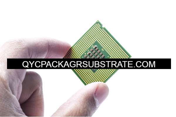
Open multi-Cavity PCB Manufacturer
Open multi-Cavity PCB Manufacturer,Open multi-cavity PCBs are specialized printed circuit boards featuring multiple cavities or cutouts within their structure. These cavities are strategically placed openings in the PCB substrate, often used to house components, reduce weight, or enhance thermal management. Open multi-cavity PCBs are designed with precise dimensions and placements to accommodate specific component requirements and optimize the overall board layout. They are utilized in applications where space efficiency, thermal dissipation, and component placement flexibility are critical, such as in aerospace, telecommunications, and high-performance computing. These PCBs contribute to improved reliability, reduced electromagnetic interference, and enhanced performance in complex electronic systems.
What is an Open multi-Cavity PCB?
An Open multi-cavity PCB refers to a printed circuit board (PCB) design that incorporates multiple cavities or openings within its structure. These cavities can be designed for various purposes such as accommodating components, creating isolated areas for different circuit sections, or for thermal management purposes.
One common application is in RF (radio frequency) and microwave circuits, where cavities are used to isolate sensitive components from electromagnetic interference (EMI) or to create resonant cavities for specific frequency operations. By incorporating multiple cavities, designers can achieve better control over signal integrity, reduce crosstalk between different parts of the circuit, and improve overall performance.
Open multi-cavity PCBs are often used in advanced electronic systems like communication equipment, radar systems, high-frequency test equipment, and aerospace applications where precise control over electromagnetic interactions and thermal dissipation is critical.
Designing and manufacturing such PCBs require expertise in CAD (computer-aided design) tools and understanding of electromagnetic field theory to optimize cavity dimensions and placements. The materials used in these PCBs are also carefully selected to ensure they meet the required electrical, mechanical, and thermal specifications for the application.
In summary, an Open multi-cavity PCB is a specialized PCB design with multiple openings or cavities strategically integrated into its structure to enhance performance, manage thermal issues, and optimize signal integrity in complex electronic systems.
Open multi-Cavity PCB Manufacturer
What are the Open multi-Cavity PCB Design Guidelines?
Designing Open multi-Cavity PCBs requires careful consideration of several key guidelines to ensure optimal performance, reliability, and manufacturability. Here are some essential guidelines:
- Cavity Placement and Size: Determine the locations and dimensions of cavities based on the specific requirements of your circuit design. Cavities should be strategically placed to minimize electromagnetic interference (EMI), reduce crosstalk, and optimize signal integrity. The size of each cavity should accommodate the components or subsystems it houses without unnecessary space that could affect PCB real estate.
- Cavity Wall Thickness: The walls of each cavity should be thick enough to provide structural integrity and prevent unwanted resonances or coupling between adjacent cavities. Generally, a thicker wall reduces coupling effects and improves EMI shielding. However, it’s essential to balance this with overall PCB weight and mechanical constraints.
- Grounding and Shielding: Proper grounding and shielding techniques are crucial in Open multi-Cavity PCB designs. Each cavity should be adequately grounded to prevent unwanted signal reflections and to maintain signal integrity. Additionally, shielding materials or techniques such as conductive coatings or metal cans may be used to further isolate sensitive components from EMI.
- Thermal Management: Consider the thermal implications of cavities on component temperature. Cavities can act as heat sinks or traps, affecting the thermal performance of the PCB. Ensure that the placement and design of cavities do not adversely impact the thermal dissipation of critical components. Heat transfer paths should be optimized to maintain operational temperatures within acceptable limits.
- Mechanical Considerations: The presence of cavities can affect the mechanical strength and rigidity of the PCB. Structural integrity should be maintained, especially if the PCB will undergo mechanical stress during assembly or operation. Reinforcements or additional supports may be necessary around cavities to prevent flexing or damage.
- Manufacturability: Design the PCB with manufacturability in mind. Ensure that cavities do not complicate the assembly process or increase production costs significantly. Consider the capabilities of your PCB manufacturer regarding cavity dimensions, tolerances, and material choices.
- EMI/EMC Compliance:Open multi-Cavity PCBs must meet electromagnetic interference (EMI) and electromagnetic compatibility (EMC) standards relevant to your application. Proper cavity design, grounding techniques, and shielding measures contribute to compliance with these regulations.
- Simulation and Testing: Use electromagnetic simulation tools to analyze the effects of cavities on signal integrity and EMI. Conduct physical testing if possible to validate simulation results and ensure the design meets performance requirements.
- Material Selection: Choose PCB materials that are suitable for Open multi-Cavity designs. Consider factors such as dielectric constant, thermal conductivity, and mechanical strength to ensure optimal performance and reliability.
- Documentation and Communication: Clearly document cavity specifications, dimensions, materials, and design considerations for communication with PCB manufacturers, assembly houses, and stakeholders. Detailed documentation helps prevent misunderstandings and ensures consistent production quality.
By adhering to these guidelines, designers can create Open multi-Cavity PCBs that effectively manage EMI, optimize signal integrity, enhance thermal performance, and meet the stringent requirements of advanced electronic applications. Each guideline plays a critical role in achieving a successful and reliable PCB design suitable for complex electronic systems.
What is the Open multi-Cavity PCB Fabrication Process?
The fabrication process for Open multi-Cavity PCBs involves several detailed steps to ensure the precise creation of cavities while maintaining overall PCB integrity and functionality. Here’s an overview of the typical fabrication process:
- Design Preparation: Begin with the PCB design phase using CAD (computer-aided design) software. Define the locations, sizes, and shapes of cavities based on the specific requirements of the circuit design and intended application. Ensure that the design includes proper grounding, shielding, and thermal management considerations for each cavity.
- Material Selection: Choose PCB materials suitable for Open multi-Cavity designs. Select base materials with appropriate dielectric properties, thermal conductivity, and mechanical strength to meet the operational requirements and ensure compatibility with cavity machining processes.
- Layer Preparation: Based on the design, prepare the PCB stack-up with appropriate layers and ensure that each layer’s dimensions and materials align with the cavity specifications. Layers may include signal, power, ground, and possibly specific layers for shielding or thermal management.
- Cavity Machining: Utilize specialized machining techniques such as mechanical milling or laser ablation to create cavities within the PCB stack-up. Machining processes must be precise to achieve the specified cavity dimensions, wall thickness, and positional accuracy relative to other features on the PCB.
- Surface Preparation: After machining cavities, ensure that the surfaces are clean and free of debris or contaminants that could affect subsequent processes such as solder mask application and component placement.
- Copper Plating and Etching: Apply copper plating to the PCB surfaces as per the design requirements. Etch away excess copper using chemical processes to define circuit traces, pads, and vias while ensuring that cavities remain unaffected by the etching process.
- Drilling and Vias: Drill holes and vias as needed to establish electrical connections between different layers of the PCB. Ensure that vias and holes do not compromise the structural integrity of the cavities or affect their functionality.
- Solder Mask Application: Apply solder mask over the PCB surfaces to protect copper traces and pads, except where electrical connections are required. Ensure that solder mask application does not obstruct cavity openings or interfere with cavity functionality.
- Silkscreen Printing: Optionally, apply silkscreen printing for component labeling and identification. Ensure that printing does not cover cavity openings or critical areas where access is needed.
- Surface Finish: Apply surface finish to protect exposed copper surfaces and ensure solderability. Common surface finishes include HASL (Hot Air Solder Leveling), ENIG (Electroless Nickel Immersion Gold), or OSP (Organic Solderability Preservative), chosen based on the application’s requirements.
- Quality Control: Perform thorough inspection and testing throughout the fabrication process. Verify cavity dimensions, tolerances, material integrity, and overall PCB functionality to ensure compliance with design specifications and quality standards.
- Final Inspection and Packaging: Conduct final inspection to confirm that the fabricated Open multi-Cavity PCB meets all requirements. Package the PCBs appropriately for protection during shipping and handling, ensuring that cavity openings are adequately protected against damage.
By following this comprehensive fabrication process, manufacturers can produce Open multi-Cavity PCBs that effectively meet the demanding requirements of advanced electronic applications, ensuring high performance, reliability, and durability in operation. Each step is critical to maintaining the integrity of cavities while achieving overall PCB functionality and quality.
How do you manufacture an Open multi-Cavity PCB?
Manufacturing an Open multi-Cavity PCB involves a series of precise steps and specialized techniques to create cavities within the PCB structure while ensuring overall integrity and functionality. Here’s a detailed overview of the manufacturing process:
- Design and CAD Preparation: Begin with the PCB design phase using CAD software. Define the locations, dimensions, and shapes of cavities based on the specific requirements of the circuit design and application. Incorporate necessary considerations for grounding, shielding, and thermal management.
- Material Selection: Choose PCB materials suitable for Open multi-Cavity designs. Select base materials with appropriate dielectric properties, thermal conductivity, and mechanical strength to meet operational requirements and machining processes.
- Layer Preparation: Prepare the PCB stack-up according to the design specifications. Ensure that each layer’s dimensions, materials, and stack sequence align with cavity requirements. Layers typically include signal, power, ground, and potentially specific layers for shielding or thermal management.
- Cavity Creation:Utilize advanced machining techniques such as mechanical milling, laser drilling, or routing to create cavities within the PCB stack-up. Machining processes must be precise to achieve exact cavity dimensions, maintain wall thickness integrity, and ensure positional accuracy relative to other PCB features.
- Surface Preparation: Clean and prepare the cavity surfaces to remove any debris, contaminants, or residues that could affect subsequent processes such as copper plating and solder mask application.
- Copper Plating and Etching: Apply copper plating to the PCB surfaces to establish conductive traces, pads, and vias according to the design. Use chemical etching processes to remove excess copper while ensuring that cavities remain unaffected and maintain structural integrity.
- Drilling and Vias: Drill holes and vias as required to establish electrical connections between different layers of the PCB. Ensure that drilling operations do not compromise cavity walls or affect their functionality.
- Solder Mask Application: Apply solder mask over the PCB surfaces to protect copper traces and pads, except where electrical connections are required. Ensure that solder mask application does not obstruct cavity openings or critical areas needing access.
- Silkscreen Printing: Optionally, apply silkscreen printing for component labeling and identification on the PCB surface. Ensure that printing does not cover cavity openings or essential areas.
- Surface Finish Application: Apply surface finish to protect exposed copper surfaces and ensure solderability. Choose appropriate surface finishes such as HASL, ENIG, or OSP based on application requirements and compatibility with cavity design.
- Quality Assurance and Testing: Conduct rigorous inspection and testing throughout the manufacturing process. Verify cavity dimensions, tolerances, material integrity, and overall PCB functionality to ensure compliance with design specifications and quality standards.
- Final Inspection and Packaging: Perform final inspection to confirm that the manufactured Open multi-Cavity PCB meets all requirements. Package the PCBs securely for protection during shipping and handling, ensuring cavity openings are adequately safeguarded against damage.
By meticulously following these manufacturing steps, PCB manufacturers can produce Open multi-Cavity PCBs that meet the stringent demands of advanced electronic applications. Each stage requires precision and attention to detail to ensure that cavities are accurately formed and integrated within the PCB structure while maintaining high reliability and performance.
How much should an Open multi-Cavity PCB cost?
The cost of an Open multi-Cavity PCB can vary widely depending on several factors, including design complexity, material choices, dimensions, quantity ordered, and the manufacturing processes involved. Here are key factors that influence the cost:
- Design Complexity: The complexity of the PCB design, including the number of cavities, their sizes, shapes, and the intricacy of the routing and layer stack-up, directly impacts the cost. More complex designs often require specialized manufacturing techniques and may involve higher engineering and setup costs.
- Materials: The choice of PCB materials significantly affects the cost. High-frequency materials, materials with specific thermal properties, or those suitable for RF applications typically cost more than standard FR-4 materials. Specialized materials may be required to meet performance specifications or environmental conditions.
- Manufacturing Processes: The specific manufacturing processes needed to create cavities, such as mechanical milling, laser drilling, or routing, contribute to the cost. Each process has associated setup costs, machining costs, and quality control measures that influence overall pricing.
- Quantity:Economies of scale apply in PCB manufacturing. Larger quantities typically result in lower unit costs due to bulk material purchases, efficient production runs, and amortization of setup costs over more units. Small prototype quantities may cost more per unit due to setup and handling charges.
- Surface Finish and Additional Features: The chosen surface finish (e.g., HASL, ENIG, OSP) and any additional features like silkscreen printing, impedance control, or special testing requirements can add to the overall cost. These features affect manufacturing complexity and may require additional processing steps.
- Quality Standards and Testing: Compliance with specific quality standards, such as IPC-A-600 for PCBs or additional testing requirements (e.g., electrical testing, thermal testing), can impact costs. Ensuring high reliability and meeting application-specific requirements may involve additional expenditures.
- Supplier and Location: The choice of PCB manufacturer and their location can influence costs due to labor rates, overhead expenses, and shipping costs. Different regions or countries may have varying cost structures for PCB manufacturing services.
Generally, for an Open multi-Cavity PCB, you can expect costs to start from several dollars per square inch for basic designs and standard materials in moderate quantities. More complex designs, specialized materials, and stringent performance requirements can increase costs significantly. It’s advisable to work closely with a PCB manufacturer to get accurate cost estimates based on your specific design and requirements. Requesting multiple quotes from different suppliers can also help in determining competitive pricing and finding the best manufacturing partner for your project.
What is Open multi-Cavity PCB base material?
The choice of base material for Open multi-Cavity PCBs depends on the specific requirements of the application, especially considering factors like frequency performance, thermal management, mechanical strength, and cost. Here are some common base materials used for Open multi-Cavity PCBs:
- FR-4 (Flame Retardant 4):FR-4 is a widely used standard PCB material due to its good electrical insulation properties, cost-effectiveness, and availability. It consists of a woven fiberglass cloth impregnated with an epoxy resin binder. FR-4 is suitable for many applications but may not be ideal for high-frequency designs or those requiring stringent thermal management.
- High-Frequency Laminates: For RF (radio frequency) and microwave applications, high-frequency laminates are used. These materials offer low dielectric constant (Dk) and low dissipation factor (Df), which are crucial for minimizing signal loss and maintaining signal integrity at high frequencies. Examples include Rogers Corporation’s RO4000 series, Taconic’s TLY series, and Isola’s Astra MT.
- Metal Core PCBs (MCPCB): These PCBs have a metal core, usually aluminum or copper, which provides excellent thermal conductivity. MCPCBs are suitable for applications requiring efficient heat dissipation, such as LED lighting, power electronics, and high-power RF amplifiers.
- Ceramic-Based PCBs: Ceramics such as alumina (Al2O3) or aluminum nitride (AlN) are used for their superior thermal conductivity compared to traditional organic PCB materials. Ceramic-based PCBs are used in high-power applications and where thermal management is critical.
- Flexible PCBs: In some cases, flexible materials such as polyimide (e.g., Kapton) or PET (polyethylene terephthalate) are used for Open multi-Cavity PCBs where flexibility or specific form factors are required.
The selection of base material for Open multi-Cavity PCBs depends on balancing electrical performance, thermal characteristics, mechanical strength, and cost considerations. Designers often choose materials based on their specific application requirements, ensuring the PCB meets performance criteria while being manufacturable within budget constraints. Consulting with a PCB manufacturer or materials supplier is recommended to select the most appropriate base material for your project’s needs.
Which company makes Open multi-Cavity PCBs?
Currently, there are many companies manufacturing Open multi-Cavity PCBs, including large electronic manufacturing services (EMS) companies and specialized PCB manufacturers. These companies typically possess advanced manufacturing equipment and skilled technical teams to meet the high-performance and reliability requirements of complex electronic systems.
In this field, our company also offers professional Open multi-Cavity PCB manufacturing services. Here are several key advantages and capabilities of our company in producing such PCBs:
- Advanced Manufacturing Equipment:We are equipped with state-of-the-art CNC machines, laser drilling equipment, and specialized PCB processing facilities. These machines can accurately fabricate complex cavity structures, ensuring that each cavity meets precise dimensional and shape requirements.
- Rich Experience and Technical Expertise: We have a highly experienced technical team proficient in PCB design, manufacturing, and assembly processes. Our engineers can provide customized solutions for Open multi-Cavity PCBs tailored to different application requirements. We maintain strict quality control and testing throughout the manufacturing process.
- Diverse Material Selection: Our company offers a variety of substrate material options, including standard FR-4, high-frequency materials (such as Rogers, Taconic, etc.), metal core boards (aluminum and copper), and ceramic substrates. These materials cater to diverse needs in electrical performance, thermal management, and mechanical strength.
- Comprehensive Quality Assurance: We adhere to ISO quality management systems and implement rigorous quality control measures throughout production. Each batch of Open multi-Cavity PCBs undergoes detailed inspection and testing to ensure compliance with customer design specifications and standards.
- Customer Support and Service: We prioritize communication and collaboration with customers, providing comprehensive technical support and after-sales service. Whether it’s initial design discussions or subsequent production requirements, we offer timely and professional support to our clients.
In summary, our company possesses the professional expertise, advanced equipment, and stringent quality control systems required for manufacturing Open multi-Cavity PCBs. Whether for complex electronic systems or high-performance PCB needs, we deliver customized solutions that meet customer requirements, ensuring product quality and timely delivery.
What are the 7 qualities of good customer service?
Good customer service is characterized by several key qualities that contribute to a positive customer experience and foster long-term relationships. Here are seven essential qualities of good customer service:
- Responsiveness: Good customer service is prompt and responsive. Customers appreciate timely assistance and quick resolution of their issues or inquiries. This includes acknowledging customer queries promptly and providing updates as necessary.
- Empathy: Empathy involves understanding and sharing the feelings of customers. Effective customer service representatives listen actively to customer concerns, acknowledge their emotions, and demonstrate genuine care and concern in their interactions.
- Clear Communication: Clear communication is crucial in customer service. Representatives should articulate information clearly and concisely, ensuring that customers understand the solutions or information provided. This includes using plain language, avoiding jargon, and verifying customer comprehension.
- Problem-Solving Skills: Good customer service involves effective problem-solving. Representatives should be able to analyze customer issues, identify solutions, and take proactive steps to resolve problems. This may involve collaboration with other departments or escalating issues as necessary.
- Product Knowledge: Knowledgeable customer service representatives inspire confidence in customers. They should have a thorough understanding of the products or services offered, including features, benefits, and troubleshooting techniques. This enables them to provide accurate information and guidance to customers.
- Professionalism: Professionalism encompasses courteous behavior, respect for customers’ time and preferences, and maintaining a positive attitude even in challenging situations. Professional customer service representatives uphold company values and strive to create a positive impression at all times.
- Consistency: Consistency is key to good customer service. Customers expect a consistent level of service across all interactions and channels. This includes uniformity in policies, response times, and the quality of assistance provided. Consistency builds trust and reliability with customers.
By embodying these qualities, organizations can deliver exceptional customer service experiences that not only meet but exceed customer expectations. Investing in training, adopting customer-centric policies, and fostering a culture of service excellence can help organizations sustain high levels of customer satisfaction and loyalty.
FAQs
What are Open multi-Cavity PCBs?
Open multi-Cavity PCBs are printed circuit boards that feature multiple cavities or openings within their structure. These cavities can be used for various purposes such as housing components, creating isolated sections for different circuits, or enhancing thermal management.
Where are Open multi-Cavity PCBs used?
Open multi-Cavity PCBs are used in applications that require precise control over EMI, thermal dissipation, and signal integrity. Common applications include RF and microwave circuits, high-frequency test equipment, aerospace electronics, and sensitive electronic systems.
How are cavities created in Open multi-Cavity PCBs?
Cavities in Open multi-Cavity PCBs are typically created using advanced machining techniques such as mechanical milling, laser drilling, or routing. These methods allow for precise shaping of cavities while maintaining structural integrity.
What materials are used in Open multi-Cavity PCBs?
The choice of materials depends on the specific application requirements. Common materials include standard FR-4 for general purposes, high-frequency laminates for RF applications, metal core PCBs for enhanced thermal management, and ceramic substrates for high-power applications.
Are Open multi-Cavity PCBs more expensive than standard PCBs?
Yes, Open multi-Cavity PCBs can be more expensive due to the additional machining processes required to create cavities, specialized materials used, and the complexity of design and assembly. However, their benefits in terms of performance and reliability often justify the cost.
How can I design an effective Open multi-Cavity PCB?
Designing an effective Open multi-Cavity PCB involves careful planning of cavity placement, size optimization, grounding strategies, and thermal management considerations. Working closely with experienced PCB designers and manufacturers is recommended to achieve optimal results.