
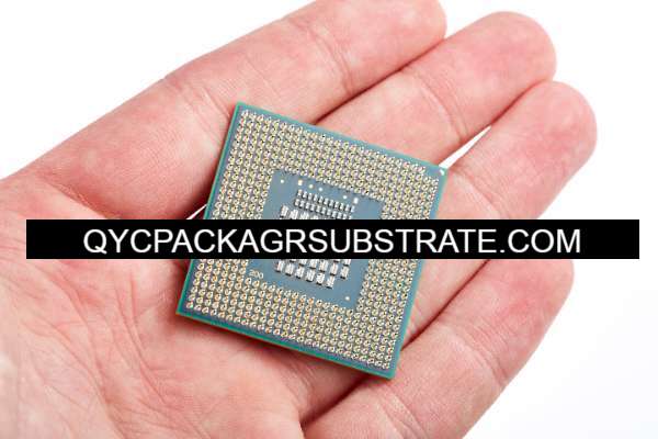
Open multi-step Cavity PCB Manufacturer
Open multi-step Cavity PCB Manufacturer,Open Multi-Step Cavity PCBs are advanced printed circuit boards featuring multiple levels of recessed cavities that are exposed or open to allow for various component placements within a single substrate. These PCBs are designed to optimize space utilization and enhance thermal management while maintaining signal integrity and reducing electromagnetic interference (EMI). Open Multi-Step Cavity PCBs are crucial for applications requiring complex electronic assemblies, such as high-performance computing, telecommunications infrastructure, and aerospace systems. They are engineered with precision to accommodate diverse component types and configurations, offering flexibility and reliability in demanding operational environments where compact design and efficient heat dissipation are essential.
What is an Open Multi-Step Cavity PCB?
An Open Multi-Step Cavity PCB refers to a specialized type of printed circuit board (PCB) that includes multiple stepped cavities integrated into its design. These cavities are strategically placed and can vary in depth and size across the board. They are typically used in applications where precise component placement and thermal management are crucial, such as high-frequency circuits, RF/microwave applications, and power electronics.
The design of Open Multi-Step Cavity PCBs allows for improved signal integrity by minimizing electromagnetic interference (EMI) and signal losses. The stepped cavities serve several purposes: they can house sensitive components, reduce crosstalk between traces, and enhance the overall thermal performance of the PCB by providing additional heat dissipation paths.
Manufacturing Open Multi-Step Cavity PCBs requires advanced PCB fabrication techniques. These include precise routing and milling processes to create the stepped features accurately. Materials chosen for these boards often include high-performance substrates like Rogers materials or other specialized laminates that offer excellent electrical properties and thermal conductivity.
Overall, Open Multi-Step Cavity PCBs are tailored solutions designed to meet specific performance requirements in demanding electronic applications, offering enhanced functionality, reliability, and performance optimization compared to traditional PCB designs.
Open multi-step Cavity PCB Manufacturer
What are the Design Guidelines for Open Multi-Step Cavity PCBs?
Designing Open Multi-Step Cavity PCBs requires careful consideration of several key guidelines to ensure optimal performance and functionality:
- Cavity Dimensions and Placement: Determine the dimensions (depth, width, length) of each cavity based on the components to be housed and the desired thermal management requirements. Ensure cavities are placed strategically to minimize signal interference and maximize thermal efficiency.
- Material Selection: Choose high-performance PCB materials with good thermal conductivity and electrical properties suitable for the application. Materials like Rogers laminates or other specialized substrates are often preferred for their excellent RF/microwave characteristics and thermal management capabilities.
- Cavity Wall Roughness: Maintain smooth cavity walls to minimize signal reflections and losses. Ensure that the surface roughness inside the cavities is within acceptable limits to prevent any adverse effects on signal integrity.
- Cavity Edge Smoothness:Smooth out the edges of the cavities to avoid sharp corners that could lead to stress concentration or affect the mechanical integrity of the board.
- Component Mounting Considerations: Plan for the mounting of components within the cavities, ensuring adequate clearance and securing methods to prevent mechanical stress or damage during operation.
- Signal Routing and Crosstalk: Carefully route signal traces around the cavities to minimize crosstalk and electromagnetic interference. Maintain appropriate clearance between traces and cavity walls to avoid signal degradation.
- Thermal Management: Utilize the cavities for effective heat dissipation by ensuring thermal vias connect to thermal pads within the cavities. This helps in conducting heat away from sensitive components and maintaining optimal operating temperatures.
- Mechanical Strength: Consider the overall mechanical strength of the PCB, especially around the cavities. Reinforce the board as needed to ensure it can withstand mechanical stresses during handling and operation.
- Testing and Validation: Conduct thorough testing and validation procedures, including simulations if necessary, to verify the performance of the PCB design. Test for thermal efficiency, signal integrity, and mechanical reliability to ensure the board meets all functional requirements.
Following these design guidelines ensures that Open Multi-Step Cavity PCBs achieve their intended performance goals, providing robust solutions for applications requiring high-frequency performance, RF/microwave capabilities, and effective thermal management.
What is the Fabrication Process for Open Multi-Step Cavity PCBs?
The fabrication process for Open Multi-Step Cavity PCBs involves several specialized steps to achieve the desired design and functionality:
- Design Preparation: Begin with detailed CAD/CAM design of the PCB layout, including the specific dimensions, placements, and configurations of the stepped cavities. This step also includes selecting the appropriate materials based on the design requirements.
- Substrate Preparation:Choose high-performance PCB substrate materials such as Rogers laminates or other specialized materials known for their excellent RF/microwave characteristics and thermal management properties. Prepare the substrate by cutting it to the required size.
- Drilling and Milling: Use precision drilling and milling machines to create the stepped cavities according to the design specifications. This step requires careful control to ensure accurate depth, width, and positioning of each cavity. The cavities are typically milled out in multiple passes to achieve smooth edges and precise dimensions.
- Copper Plating: Apply copper plating to the substrate surface to create the conductive pathways and pads necessary for component mounting and signal routing. This involves cleaning the substrate, applying a thin layer of copper through electroplating, and then etching away the excess copper to leave behind the desired circuit patterns.
- Inner Layer Imaging and Lamination: Use photolithography and etching techniques to define the inner layer circuitry. Apply photoresist, expose it to UV light through a mask of the circuit pattern, develop the exposed photoresist, and etch away the unwanted copper. Repeat this process for each layer of the PCB as needed. After etching, laminate the layers together under heat and pressure to form a multilayer structure.
- Outer Layer Imaging and Plating: Repeat the imaging and plating process for the outer layers of the PCB to complete the circuitry and provide external connections.
- Solder Mask Application: Apply solder mask over the entire PCB surface, leaving only the areas for soldering components exposed. The solder mask protects the copper traces from oxidation and facilitates soldering during assembly.
- Surface Finish: Apply a surface finish to protect the exposed copper surfaces and enhance solderability. Common surface finishes include HASL (Hot Air Solder Leveling), ENIG (Electroless Nickel Immersion Gold), and OSP (Organic Solderability Preservatives).
- Silkscreen Printing: Optionally, add component designators, logos, and other markings using silkscreen printing for identification and assembly guidance.
- Final Inspection and Testing: Conduct thorough inspection and testing to verify the quality and functionality of the Open Multi-Step Cavity PCB. This includes electrical testing, dimensional verification, and possibly thermal testing to ensure it meets all specified requirements.
- Assembly: Finally, assemble components onto the PCB using automated or manual assembly processes, depending on the complexity and volume of production.
By following these steps with precision and attention to detail, manufacturers can produce Open Multi-Step Cavity PCBs that meet the demanding requirements of high-frequency applications, RF/microwave circuits, and advanced thermal management solutions.
How do you Manufacture an Open Multi-Step Cavity PCB?
Manufacturing an Open Multi-Step Cavity PCB involves a series of detailed steps to achieve precise cavity dimensions, optimal thermal management, and high-performance electrical characteristics:
- Design and Material Selection: Begin with CAD/CAM design software to layout the PCB, specifying cavity dimensions, placements, and material selection. Choose high-performance substrates like Rogers laminates known for RF/microwave properties and thermal conductivity.
- Substrate Preparation:Cut the substrate material to size according to design specifications, ensuring it meets the dimensional requirements for the PCB.
- Drilling and Milling: Use precision CNC machines to drill and mill the stepped cavities into the substrate. This process requires multiple passes to achieve accurate depth, width, and smooth edges for each cavity.
- Copper Plating: Apply copper plating onto the substrate surface to create conductive pathways and pads for component mounting and signal routing. Electroplate a thin layer of copper, then etch away excess copper to form the desired circuit patterns.
- Inner Layer Processing:Apply photoresist to define inner layer circuitry using photolithography. Expose the photoresist to UV light through a mask of the circuit pattern, develop it, and etch away the exposed copper. Repeat for each inner layer of the multilayer PCB.
- Lamination:Stack and laminate the inner layers together under heat and pressure, bonding them into a single multilayer structure. This process ensures electrical connectivity between layers.
- Outer Layer Processing:Repeat the imaging and plating process for the outer layers to complete the circuitry and provide external connections.
- Solder Mask Application: Apply solder mask over the entire PCB surface, leaving exposed areas for soldering components. The solder mask protects copper traces from oxidation and aids in soldering during assembly.
- Surface Finish: Apply a surface finish like HASL, ENIG, or OSP to protect exposed copper surfaces and enhance solderability.
- Silkscreen Printing: Optionally, apply silkscreen printing to add component designators, logos, and other markings for assembly guidance and identification.
- Final Inspection and Testing: Conduct thorough inspection and testing to verify PCB quality and functionality. This includes electrical testing, dimensional verification, and possibly thermal testing to ensure it meets specifications.
- Component Assembly: Finally, assemble components onto the PCB using automated or manual methods. Ensure components are securely mounted within the cavities and soldered correctly to the PCB.
By meticulously following these manufacturing steps, manufacturers can produce Open Multi-Step Cavity PCBs that excel in high-frequency applications, RF/microwave circuits, and thermal management, meeting stringent performance requirements.
How much should an Open Multi-Step Cavity PCB cost?
The cost of an Open Multi-Step Cavity PCB can vary widely based on several factors:
- Complexity of Design: The number and depth of cavities, as well as the complexity of the layout and routing, significantly impact costs. More complex designs require more precise milling and drilling, which increases manufacturing costs.
- Materials Used: High-performance materials such as Rogers laminates or other specialized substrates with enhanced electrical and thermal properties tend to be more expensive than standard FR4 materials.
- Production Volume: Economies of scale apply—higher quantities typically reduce per-unit costs due to efficiencies in manufacturing and setup.
- Additional Processes: Surface finish options (e.g., HASL, ENIG), solder mask types, and any additional requirements such as impedance control or special testing can add to the overall cost.
- Manufacturer and Location: Different PCB manufacturers have varying cost structures based on their equipment, expertise, and geographic location.
To provide a rough estimate, Open Multi-Step Cavity PCBs generally cost more than standard PCBs due to their specialized design and manufacturing requirements. Prices can range from tens to hundreds of dollars per board, depending on the above factors. For a precise quote, it’s advisable to consult with PCB manufacturers, providing them with detailed design specifications and expected production volumes. This allows for accurate cost assessments tailored to specific project needs.
What is the Base Material for Open Multi-Step Cavity PCBs?
The base material for Open Multi-Step Cavity PCBs typically consists of high-performance substrates that offer excellent electrical and thermal properties. Some common base materials used include:
- Rogers Laminates: Rogers Corporation offers a range of high-frequency laminates known for their low dielectric constant (εr) and low loss tangent (tanδ), making them ideal for RF/microwave applications where signal integrity is critical.
- Isola FR408HR:This material combines a low dielectric constant and loss factor with enhanced thermal performance, suitable for high-speed digital and high-frequency designs.
- Taconic TLY-5: Taconic’s TLY series laminates provide high thermal conductivity and mechanical stability, making them suitable for applications requiring efficient heat dissipation.
- Arlon AD Series: Arlon’s AD series laminates offer high thermal conductivity and reliability, designed for demanding RF/microwave applications.
These materials are chosen for their ability to support the precise milling and drilling required for stepped cavities, as well as their capability to manage heat effectively. They also provide the electrical characteristics necessary for high-frequency performance and signal integrity in Open Multi-Step Cavity PCB designs. The specific choice of base material depends on the application requirements, including frequency range, thermal management needs, and performance specifications.
Which companies manufacture Open Multi-Step Cavity PCBs?
Currently, companies manufacturing Open Multi-Step Cavity PCBs primarily include well-known enterprises specializing in high-performance electronic components and packaging solutions. These companies typically possess advanced manufacturing equipment and extensive technical expertise to meet the design and production requirements of complex circuit boards.
- Rogers Corporation: Rogers Corporation is a global leader in high-performance materials, offering a variety of advanced laminates for RF/microwave applications. Their materials are widely used in the manufacturing of Open Multi-Step Cavity PCBs to support high-frequency, low-loss, and excellent thermal management performance.
- Isola Group: Isola Group provides a broad range of high-performance laminate materials, including FR408HR, suitable for high-speed digital and high-frequency circuit designs. Their materials play a significant role in the manufacturing of Open Multi-Step Cavity PCBs, supporting complex circuit layouts and precise machining.
- Taconic Advanced Dielectric Division: Taconic’s TLY series laminates are renowned for their excellent thermal conductivity and mechanical stability, particularly suitable for applications requiring effective heat dissipation, including the production of Open Multi-Step Cavity PCBs.
- Arlon Electronic Materials: Arlon Electronic Materials’ AD series laminates offer high thermal conductivity and reliability, designed for high-frequency RF/microwave applications, supporting the high-performance requirements of complex circuit boards.
Our company is also capable of manufacturing Open Multi-Step Cavity PCBs. We possess advanced production equipment and a skilled technical team dedicated to meeting customer demands for high-performance circuit boards. We provide customized design and manufacturing solutions, including precise drilling and milling processes and the selection of high-performance materials. We are committed to ensuring every PCB meets customer technical specifications and quality standards through rigorous quality control and testing processes. Whether in RF/microwave applications, high-frequency circuit design, or thermal management, we offer reliable solutions to meet various application needs.
What are the 7 Qualities of Good Customer Service?
Good customer service is characterized by several key qualities that contribute to a positive customer experience and build strong relationships. Here are seven essential qualities:
- Responsiveness: Good customer service involves promptly addressing customer inquiries, concerns, and requests. This responsiveness shows customers that their needs are valued and helps in resolving issues efficiently.
- Empathy: Empathy is crucial in understanding and sharing the feelings of customers. It involves listening actively to their concerns, acknowledging their emotions, and showing genuine concern for their experience.
- Clear Communication: Effective communication is essential in customer service. Clear and concise communication helps in providing information, answering questions, and ensuring customers understand the resolutions or next steps.
- Product Knowledge: Good customer service representatives are knowledgeable about the products or services they support. This knowledge enables them to provide accurate information, offer helpful recommendations, and troubleshoot effectively.
- Problem-Solving Skills: Customers often seek assistance when facing challenges. Strong problem-solving skills allow customer service teams to analyze issues, explore solutions, and resolve problems efficiently, ensuring customer satisfaction.
- Professionalism: Professionalism in customer service involves maintaining a positive attitude, staying calm under pressure, and treating customers with respect and courtesy at all times. It builds trust and enhances the customer’s overall experience.
- Follow-Up: Following up with customers after resolving an issue or completing a transaction demonstrates commitment to their satisfaction. It ensures that customers feel valued and helps in addressing any lingering concerns or feedback.
These qualities collectively contribute to creating a positive customer service experience, fostering loyalty, and enhancing the reputation of the organization.
FAQs about Open Multi-Step Cavity PCBs
What are Open Multi-Step Cavity PCBs?
Open Multi-Step Cavity PCBs are specialized printed circuit boards that feature multiple stepped cavities integrated into their design. These cavities are used for housing components, reducing electromagnetic interference (EMI), and enhancing thermal management in high-frequency and RF/microwave applications.
What materials are used in Open Multi-Step Cavity PCBs?
High-performance materials such as Rogers laminates, Isola FR408HR, Taconic TLY series, and Arlon AD series are commonly used. These materials offer excellent electrical properties and thermal conductivity.
What industries use Open Multi-Step Cavity PCBs?
Industries include telecommunications, aerospace, defense, medical devices, and any application requiring high-frequency circuitry, RF/microwave capabilities, and efficient thermal management.
How are Open Multi-Step Cavity PCBs manufactured?
Manufacturing involves precise drilling and milling of stepped cavities into high-performance substrates. These cavities are then integrated into the PCB design to accommodate components and improve performance.
What factors affect the cost of Open Multi-Step Cavity PCBs?
Cost factors include the complexity of design, materials used, production volume, additional processes like surface finish and testing, and the manufacturing capabilities of the supplier.
Where can I get Open Multi-Step Cavity PCBs manufactured?
Several specialized PCB manufacturers and suppliers offer production services for Open Multi-Step Cavity PCBs. Companies with expertise in high-frequency PCBs and RF/microwave applications are typically best suited for these requirements.