
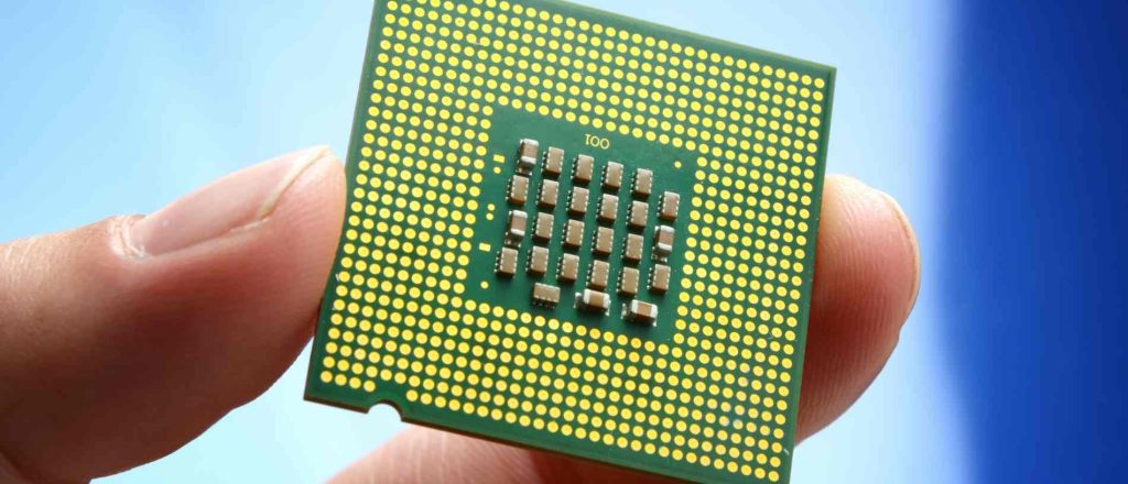
IC/BGA substrate manufacture. we can produce the best samllest bump pitch with 100um, the best smallest trace are 9um. and the smallest gap are 9um. most of the design are 15um to 30um trace and spacing. In the ever-evolving realm of modern electronics, substrate design stands as a cornerstone technology. But what exactly is substrate design? At its core, substrate design is the art and science of crafting the backbone of electronic devices. It encompasses the creation of printed circuit boards (PCBs), the heart and soul of electronic circuits. These intricate boards house and interconnect the electronic components that power our gadgets and machinery.
The significance of substrate design in modern electronic devices cannot be overstated. It is the unsung hero, the unsung hero that quietly empowers the digital world we live in. PCBs, and by extension, substrate design, are the unsung heroes that silently drive the smartphones in our pockets, the laptops on our desks, and the smart devices that streamline our lives. Without substrate design, our world would be devoid of the digital marvels we often take for granted.
Key Features of Substrate Design
Material Selection
1.Pros and Cons of Different Materials The choice of material can significantly impact the performance and durability of the substrate.
FR-4: This commonly used material offers excellent electrical insulation and cost-effectiveness. However, it might not be suitable for high-frequency applications due to its dielectric properties.
Rogers: Known for its high-frequency capabilities, Rogers material excels in signal integrity but tends to be more expensive.
Polyimide: This flexible material is great for applications requiring bendability, such as flexible PCBs. However, it may not handle high temperatures as well as other materials.
2.How to Choose the Right Material Selecting the appropriate material for your substrate design involves a thorough evaluation of your project requirements. Consider factors like frequency, thermal tolerance, and flexibility. A few steps to make the right choice include:
Understanding the specific needs of your project.
Analyzing the electrical and thermal properties of materials.
Weighing the cost-effectiveness against the performance requirements.
Layer Structure
The layer structure of a substrate is another critical aspect that deserves attention. Let’s compare multi-layer and double-layer substrates and explore the advantages of a multi-layer design:
Comparing Multi-Layer and Double-Layer Substrates
Double-Layer Substrate: This design features two layers of material with copper traces on each side. It is suitable for simple circuits but can be limiting for complex designs.
Multi-Layer Substrate: This approach involves multiple layers stacked together, allowing for more complex and compact circuits. It’s ideal for high-density applications.
Advantages of a Multi-Layer Design
The choice between double-layer and multi-layer designs often boils down to project complexity and requirements. Multi-layer designs offer several advantages, such as:
Higher Component Density: Multi-layer substrates allow for more components to be integrated into a smaller space.
Improved Signal Integrity: With multiple layers, it’s easier to separate signal and power lines, reducing interference.
Enhanced Thermal Management: More layers provide better heat dissipation, vital for high-power applications.
Routing Layout
Proper routing layout is essential for optimizing the performance of a substrate. Let’s explore optimal layout strategies and the delicate balance between signal integrity and noise immunity:
Optimal Layout Strategies
Achieving an optimal routing layout involves careful planning to minimize signal interference and noise. Some strategies include:
Shorter Traces: Reducing the length of traces minimizes signal delays and susceptibility to noise.
Ground Planes: Effective use of ground planes helps with signal return paths and shielding against electromagnetic interference.
Signal Separation: Keep sensitive analog and digital signals physically separate to reduce crosstalk.
Balancing Signal Integrity and Noise Immunity
Balancing signal integrity and noise immunity is a continuous process during substrate design. Engineers must strike a balance that ensures data transmission quality while reducing the risk of interference. This involves:
Properly placed decoupling capacitors to suppress voltage fluctuations.
Careful consideration of trace impedance and transmission line effects.
Regular testing and simulation to fine-tune the layout.
Understanding these key features of substrate design is essential for creating high-performance electronic devices in various industries, from smartphones to automotive and medical applications. The right material, layer structure, and routing layout are fundamental in achieving the desired functionality and reliability of the end product.
Manufacturing Process
Printed Circuit Board (PCB) Manufacturing Flow
Design
In the realm of substrate design, the process begins with meticulous design. Engineers and designers carefully craft the layout of the PCB. The design phase is a critical juncture where material selection, layer structure, and routing layout are considered. The aim is to create a blueprint that optimizes signal flow, minimizes interference, and meets the specific needs of the end product.
Printing
Once the design is finalized, it’s time to bring it to life. Printing is a key step in PCB manufacturing, where the circuit pattern is transferred onto the substrate material. This is done with precision and attention to detail, ensuring that the conductive pathways are accurately reproduced.
Chemical Etching
The chemical etching stage involves selectively removing unwanted copper from the substrate. This step is crucial for shaping the conductive pathways according to the design specifications. Chemical etching ensures that the circuit connections are well-defined, allowing for the precise transmission of electrical signals.
Lamination After etching, multiple layers of the PCB are carefully stacked and laminated together. The layer structure, as discussed earlier, plays a vital role in determining the PCB’s functionality. Lamination secures the layers and ensures they are well-bonded, providing stability and durability to the final product.
Advanced Technologies
Challenges of Ultra-Thin Substrates
As electronic devices continue to shrink in size and increase in complexity, the demand for ultra-thin substrates has surged. These substrates come with their unique set of challenges. Manufacturing ultra-thin substrates requires an exceptionally high level of precision and control to avoid issues like warping, bending, or even structural failure. Advanced techniques are employed to handle these challenges, ensuring the reliability of these ultra-thin substrates.
Latest Manufacturing Trends and Technologies
To stay at the forefront of substrate design, manufacturers are continually embracing cutting-edge technologies. This includes the use of advanced materials, such as flexible substrates, to cater to emerging applications like foldable smartphones. Furthermore, the industry is increasingly adopting environmentally friendly manufacturing practices. New methods for recycling and reducing waste are being explored, aligning with the growing emphasis on sustainability in electronics production.
In summary, the manufacturing process of printed circuit boards (PCBs) is a multifaceted procedure that involves careful design, precise printing, controlled chemical etching, and secure lamination. In the ever-evolving landscape of substrate design, addressing challenges related to ultra-thin substrates and adopting the latest manufacturing trends and technologies is essential to meet the demands of modern electronic devices.
Application Areas
Substrate design plays a pivotal role in a wide array of application areas, each with its own unique demands for performance and reliability. Let’s delve deeper into these domains where substrate design makes a substantial impact:
Electronics Products
Smartphones: In the world of smartphones, where sleek designs and high functionality are paramount, substrate design becomes critical. The compact form factor necessitates multi-layer substrates to accommodate various components while maintaining signal integrity. Substrate materials with good heat dissipation properties are essential, considering the high-performance processors and graphics chips used in modern smartphones.
Laptops: Laptops, like smartphones, demand efficient use of space. The substrate design in laptops needs to strike a balance between size and functionality. Multi-layer PCBs enable the integration of processors, memory, and connectivity components. As laptops become thinner and more powerful, substrate design must adapt to meet the evolving requirements of these portable computing devices.
Automotive Industry
In-vehicle Electronic Systems: The modern automobile is a technological marvel with a myriad of electronic systems, from infotainment and navigation to engine management and safety features. Substrate design in this context focuses on ruggedness, resistance to vibration and temperature extremes, and high reliability. Multi-layer substrates are employed to accommodate the complexity of these systems, ensuring efficient signal routing and reduced interference.
Autonomous Driving Technology: The advent of autonomous driving relies heavily on advanced sensor technology, and substrate design is integral to the sensors’ functionality. Lidar, radar, and camera modules rely on well-designed substrates for accurate data processing. These substrates must provide high-speed data transmission while withstanding harsh environmental conditions.
Medical Devices
Pacemakers: Life-saving medical devices like pacemakers rely on substrate designs that prioritize low power consumption and miniaturization. The substrate must provide a reliable platform for the device’s electronic components, ensuring long-lasting performance without the need for frequent battery replacements.
Imaging Equipment: Medical imaging equipment, such as MRI and CT scanners, demands substrates capable of handling high-frequency signals and maintaining signal integrity. These substrates must also minimize interference to produce clear, accurate images. Advances in substrate design contribute to more precise diagnostic capabilities and patient safety.
In all these application areas, the choice of substrate material, layer structure, and routing layout plays a crucial role in the performance, durability, and functionality of the end product. Substrate design is a dynamic field that continually adapts to the evolving requirements of these diverse industries, ensuring that electronic systems operate efficiently and reliably in various challenging environments.
Optimization and Future Outlook
Google Search Engine Optimization (SEO)
In today’s digital age, enhancing the visibility of your substrate design products is paramount.
1.Enhancing Product Visibility through SEO: Implementing effective SEO strategies can involve optimizing your website content, meta descriptions, and keywords. By using relevant and high-ranking keywords related to substrate design, you can increase the chances of your products appearing at the top of search results. This not only ensures a broader reach but also positions your offerings as the go-to choice in the field.
Future Trends
The world of substrate design is continually evolving, driven by technological advancements and a growing emphasis on sustainability. As we look ahead, two significant aspects will shape the future landscape:
1.Impact of Advanced Technologies: With each passing year, technology continues to push the boundaries of what is possible in substrate design. Miniaturization, high-speed data transmission, and material innovations are driving the industry forward. The integration of cutting-edge technologies into substrate design will redefine the capabilities of electronic devices and their applications. Keeping pace with these advancements will be essential for staying competitive in the market.
2.Development of Eco-Friendly Substrate Designs: Sustainability has become a central concern for many industries, including electronics. The future of substrate design will see a strong emphasis on eco-friendly materials and processes. As society becomes more environmentally conscious, products with minimal environmental impact will gain a competitive edge. Manufacturers will need to adapt by exploring alternative materials, reducing waste, and adopting greener production methods to meet the demands of eco-conscious consumers.
In summary, optimizing your substrate design products for online visibility through SEO is crucial in today’s digital landscape. Simultaneously, staying attuned to the impact of advanced technologies and embracing eco-friendly substrate designs will be key to thriving in the evolving world of electronic components.