
We are a professional packaging substrate supplier, we mainly produce ultra-small bump pitch substrate, ultra-small trace and spacing packaging substrate and PCBs. Not only do we provide high-quality products, we are also committed to providing excellent technical support and customer service. Our professional team is ready to solve your technical problems and ensure your project goes smoothly. When you choose our Packaging Substrate, you choose superior performance and worry-free backing.
Advanced semiconductor packaging substrate
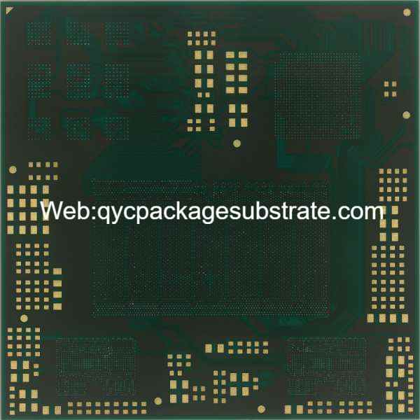
Advanced semiconductor packaging substrates are a key component in semiconductor packaging technology and are used to support, connect and protect semiconductor components on the chip. These substrates play an important role in modern electronic devices and chip packaging, especially in high-performance and complex applications.
Basic functions
Semiconductor packaging s
ubstrates mainly have two basic functions. First, they provide a mechanical support structure that holds the chip in the package to prevent physical damage. Second, they provide electrical connections to the semiconductor components on the chip, connecting the chip to external circuitry.
Materials
These substrates are usually made of high-performance materials such as Si, GaN, AlN or ceramics. Material selection depends on application requirements such as thermal conductivity, electrical properties and packaging environment.
Multi-layer structure
In complex applications, semiconductor packaging substrates often adopt multi-layer structures. These multiple layers include electrical, insulating, and thermal layers to ensure reliable transmission of electrical signals, isolation, and thermal performance.
Electrical connections
Electrical connections on a substrate typically consist of wires, pads, connections, and electrical traces that connect the pins on the chip to external circuitry. These connections must meet high-frequency signal transmission and low signal-to-noise ratio requirements.
Heat dissipation performance: High-performance semiconductor packaging substrates also have excellent heat dissipation properties to effectively dissipate the heat generated by the chip and prevent overheating from damaging semiconductor components.
Technological Advances
Advanced semiconductor packaging substrates are an area that continues to evolve to meet the needs of new generations of chips and electronic devices. New technologies include higher-density interconnects, better heat-dissipation materials, more refined manufacturing processes, and three-dimensional stacking of packaging substrates.
Application fields
Advanced semiconductor packaging substrates play a key role in fields such as high-performance computing, communication equipment, automotive electronics, artificial intelligence, and the Internet of Things, as these fields require higher performance and reliability of semiconductor components.
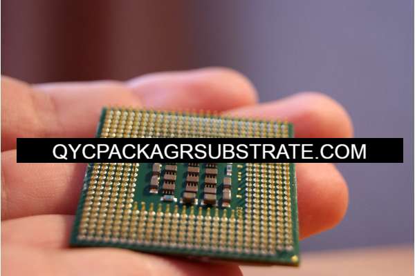
What is a Package Substrate?
“Package substrate” is a term widely used in the fields of electronic engineering and electronics manufacturing, often used to refer to the base plate used for IC packaging of electronic components. Its main function is to provide mechanical support, electrical connections and heat dissipation to protect and connect integrated circuit chips.
The following is a detailed introduction to the packaging substrate:
Mechanical support
Package substrates are often made of strong materials such as ceramics, resins, or metals to provide mechanical support. This helps protect the chip from physical damage such as vibration, shock and pressure.
Electrical connections
The package substrate is usually integrated with wires, solder joints, and connectors to connect the chip and other electronic components to the circuit board or circuit system. These connections can be solder joints, sockets, connectors or other electrical connection technology.
Heat dissipation
Some package substrates are also designed with heat dissipation functions to help the chip cool down during operation. High-performance integrated circuits may generate large amounts of heat, which may affect their performance and lifespan if not properly dissipated. Thermal design can include heat sinks, thermal pads, thermally conductive materials, etc.
Packaging type
There are many types of packaging substrates, including double-sided substrates, multi-layer substrates and flexible substrates. Each type is suitable for different applications and needs. For example, multilayer substrates have multiple layers to accommodate more electrical connections and signal layers, while flex substrates are made of flexible materials and are suitable for curved or curved applications.
Package Size
The size and shape of the package substrate can be customized to meet the needs of a specific application. Some package substrates are small and suitable for micro packages, while other package substrates are larger and suitable for large packages.
Packaging substrates process capability
Packaging substrate process capability refers to the manufacturer’s ability to ensure that the product meets certain standards and specifications during the production process of packaging substrates. It covers many aspects, including process control, quality management, technical capabilities and innovation capabilities, etc.
Process control
The manufacturing process of packaging substrates requires strict control of the process, including raw material selection, production equipment operation, process parameter control, etc. Good process control can ensure the stability and reliability of product quality.
Quality management
Quality management is crucial in the packaging substrate process, involving the entire process control from raw material procurement to finished product delivery. It includes quality testing, quality control and quality improvement, etc., aiming to ensure that products meet specification requirements and provide stable and reliable performance.
Technical capabilities
Packaging substrate manufacturing requires a high level of technical capabilities, including expertise in materials science, process engineering, equipment technology, etc. Manufacturers need to constantly update technology to respond to changes in market demand and provide competitive products.
Innovation capabilities
Packaging substrate process capabilities also require continuous innovation capabilities to adapt to evolving market demands and the emergence of new technologies. This may involve the application of new materials, the development of new processes, and the design of new products to improve product performance and competitiveness.
Sustainable development capabilities
In today’s context of concern about environmental protection and sustainable development, packaging substrate process capabilities also include meeting environmental protection requirements and paying attention to sustainable development. Manufacturers need to focus on energy conservation, emission reduction, waste disposal and environmental protection to meet social requirements for environmental protection.
Price and delivery date of packaging substrate
Price: The price of packaging substrates refers to the monetary cost of purchasing those substrates. Price can be affected by a variety of factors, including but not limited to the following:
Quantity: Generally speaking, purchasing higher quantities of package substrates may result in greater discounts, as production costs typically decrease with higher volume. The higher the quantity purchased, the lower the cost per substrate is likely to be
Specifications and quality: Package substrates of different specifications and quality may have different prices. High-performance, high-quality substrates typically cost more.
Suppliers: Different suppliers may have different pricing strategies, so prices will vary from supplier to supplier. Sometimes, suppliers with a long history of cooperation may offer more competitive prices.
Special customization needs: If a custom packaging substrate is required, such as special dimensions, materials or processes, this will usually result in a higher price as it requires additional engineering and production costs.
Packaging Substrate
Delivery Date: The delivery date is the date when the package substrate will be delivered to the buyer. This date is usually clearly defined in the purchase contract, which is an agreement between the supplier and the buyer. Delivery dates are affected by:
Stock Availability: If the package substrate is available in the supplier’s inventory, the delivery date may be faster. But if customization or high-volume production is required, the delivery date may be delayed.
Production Time: The time required to produce a package substrate affects delivery dates. Production time is affected by order quantity, process complexity and production capacity.
Shipping Time: Delivery dates are also affected by the shipping time required from supplier to buyer. This may vary based on geographic location and shipping method.
Urgent demand: If the buyer has urgent demand, expedited production and delivery may be required, but this usually comes with additional costs.
The material type of the packaging substrate
The material type of the packaging substrate is critical to the semiconductor packaging process because different material types have different properties.
Organic substrate
FR-4: FR-4 is a common organic substrate material commonly used in electronic circuit board manufacturing. It has good electrical insulation properties and mechanical strength.
Polymer materials: Polymer materials such as PI and PTFE are also used as packaging substrate materials. They have excellent high temperature stability and electrical properties.
Ceramic substrate
Alumina: Aluminum oxide is a common ceramic substrate material with excellent thermal conductivity and electrical insulation properties. It is commonly used in high-power semiconductor packaging such as power amplifiers and high-frequency radio frequency circuits.
Silicon Nitride: Silicon nitride substrates offer excellent thermal conductivity and are suitable for high temperature and high power applications.
Metal substrate
Aluminum substrate: Aluminum substrate is a metal substrate with good thermal conductivity and is usually used for packaging of high-power heating components, such as LED lights and power semiconductor devices.
Copper Substrate: Copper substrate is commonly used in high-frequency RF circuits because of its excellent electrical conductor properties.
Composite materials
Metal-organic composites: These substrates combine metallic and organic layers to provide excellent thermal conductivity and mechanical strength while retaining electrical insulation properties. This is useful for high-density electronic packaging.
Flexible substrate
Polyester film: Flexible substrates are often made from polyester film, a material that is very thin and flexible and suitable for applications that require curved or curved designs, such as flexible electronics.
Other types of materials: For example, brand: Showa Denko brand base materials, they are MCL-E-705G, MCL-E-770G, MECL-E-700G, MECL-E-795G and others. And Ajinonoto brand base materials. The are GX92R, GXT31R2, GZ41R2H, GL102R8HF,GL103R8H and others. Most this base materials are for High multilayer Packaging Substrates. About the Soldermask layers. They are SR7300G, PSR-4000 AUS703, PSR-800 AUS SR1 and other types. Surface finishing are ENEPIG , IT, ENEPIG+SOP, IT+SOP, Thin Ni ENEPIG, and others.
If you have any questions, please feel free to contact us and we will reply to you as soon as possible. It is our pleasure to help you.
Where can I buy high quality packaging substrates
If you need to buy high quality packaging substrates, you can trust us completely. We are SHENZHEN QYC CO.,LTD, a company specializing in the production of Flip Chip Package Substrate. We have more than 10,000 employees and use high-precision equipment from Japan to manufacture FC BGA Substrate, so the quality of our products is very stable.
Our company can manufacture Flip Chip Package Substrate from 4 to 18 layers with minimum line width and minimum pitch of 9 microns. For example, we can provide Flip Chip Package Substrate in high quality 14-layer ABF material. Most notably, our production turnaround is very fast, typically taking only 1 to 2 months, ensuring your project moves forward quickly.
In addition, we have many different types of Package Substrate materials, which are mainly from Japan, South Korea, Taiwan and China. We will carefully select the appropriate materials to produce Substrate according to your specific needs to ensure that you are satisfied project requirements.
If you have further questions or require more information about our products and services, please feel free to contact us. We look forward to working with you and providing you with high-quality Flip Chip Package Substrate to meet your project needs.