
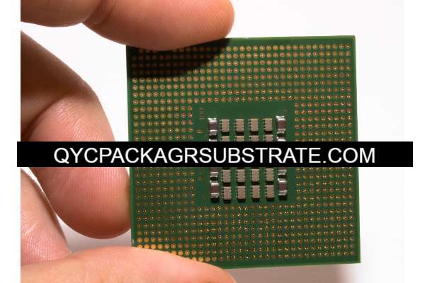
What is PGA Package Substrate?
PGA Package Vender and PGA Package Substrate Supplier, We do the package service and we also produce ultra-small bump pitch substrate, ultra-small trace and spacing packaging substrate and microtrace HDI PCBs.
The PGA (Pin Grid Array) package substrate is a type of integrated circuit (IC) packaging technology used in computer processors and other semiconductor devices. It consists of a grid of pins arranged in a uniform pattern on the underside of the chip package. These pins are used to connect the chip to the motherboard or other electronic components.
PGA packages are popular for CPUs (Central Processing Units) and other high-performance integrated circuits because they offer good electrical performance, thermal dissipation, and reliability. The PGA substrate typically consists of a ceramic or organic material that provides mechanical support and electrical insulation for the chip.
One of the key advantages of PGA packages is their robustness and ease of handling during manufacturing and assembly processes. However, they may require more space on the motherboard compared to other packaging technologies such as BGA (Ball Grid Array) or LGA (Land Grid Array).
Overall, PGA package substrates play a crucial role in providing electrical connectivity and mechanical support for integrated circuits, particularly in high-performance computing applications.
PGA Package Substrate
What are the functions of PGA Package Substrate?
The functions of PGA Package Substrate include:
Providing Mechanical Support: The PGA substrate offers a stable platform for the chip, ensuring it remains undamaged during use and transportation.
Facilitating Electrical Connections: The pins on the PGA substrate establish electrical connections between the chip and the motherboard or other electronic devices. These pins transmit signals, data, and power, enabling the chip to communicate with other components effectively.
Thermal Management: PGA substrates are often designed for heat dissipation, ensuring that the chip maintains an appropriate operating temperature under high loads. Effective thermal management extends the chip’s lifespan and enhances its performance.
Electrical Insulation: The material of the PGA substrate provides electrical insulation for the chip, preventing circuit shorts or other electrical issues.
Ease of Manufacturing and Assembly: PGA packaging is typically easier to manufacture and assemble compared to other packaging technologies, making the production process more efficient.
Overall, PGA Package Substrate plays a crucial role in ensuring chip reliability, providing electrical connectivity, and managing thermal conditions, making it an integral component of many integrated circuit devices.
What are the different types of PGA Package Substrate?
There are several different types of PGA (Pin Grid Array) package substrates, each with its own characteristics and applications. Some common types include:
Ceramic PGA (CPGA): CPGA substrates are made of ceramic material, which provides excellent electrical insulation and thermal conductivity. These substrates are often used in high-performance applications where thermal management is critical.
Plastic PGA (PPGA): PPGA substrates are made of plastic material, which is less expensive than ceramic but offers adequate electrical insulation and mechanical support. These substrates are commonly used in consumer electronics and low-power applications.
Flip-Chip PGA (FCPGA): FCPGA substrates feature a flip-chip design where the chip is mounted face-down onto the substrate. This configuration allows for shorter electrical paths and improved electrical performance, making it suitable for high-speed applications such as microprocessors.
Staggered PGA (SPGA): SPGA substrates have pins arranged in a staggered pattern rather than a regular grid, allowing for higher pin densities and more compact packaging. These substrates are used in applications where space is limited, such as in mobile devices.
Cavity Down PGA (CDPGA): CDPGA substrates feature a cavity on the substrate where the chip is mounted, allowing for better thermal management by providing direct contact with a heat sink or thermal interface material.
These are just a few examples of PGA package substrates, and there may be other specialized types designed for specific applications or requirements. The choice of substrate type depends on factors such as performance requirements, cost considerations, and form factor constraints.
What is the relationship between PGA Package Substrate and IC packaging?
The PGA (Pin Grid Array) Package Substrate is a specific type of substrate used in integrated circuit (IC) packaging. IC packaging encompasses the various methods and technologies used to protect and connect semiconductor chips or dies to the outside world. PGA Package Substrate is one of these packaging methods.
Here’s the relationship between PGA Package Substrate and IC packaging:
Component of IC Packaging: The PGA Package Substrate is a critical component of IC packaging. It provides the mechanical support, electrical connections, and sometimes thermal management for the semiconductor chip.
Electrical Connectivity: The PGA Package Substrate facilitates electrical connections between the semiconductor chip and other components, such as a motherboard or printed circuit board (PCB). The pins on the PGA substrate form the interface through which electrical signals, data, and power are transmitted.
Mechanical Support: The substrate offers physical support to the semiconductor chip, protecting it from mechanical stresses and preventing damage during handling, assembly, and operation.
Thermal Management: In some cases, PGA Package Substrates are designed to aid in thermal management by dissipating heat generated by the semiconductor chip. This can help maintain optimal operating temperatures and prolong the life of the chip.
In summary, the PGA Package Substrate is an integral part of the IC packaging process, providing essential functions such as electrical connectivity, mechanical support, and thermal management for semiconductor chips. It represents one of the many packaging options available in the field of semiconductor technology.
How does PGA Package Substrate differ from PCB?
The PGA (Pin Grid Array) Package Substrate and PCB (Printed Circuit Board) serve different purposes in electronic devices, although they both play important roles in facilitating connections between components. Here’s how they differ:
Function:
PGA Package Substrate: The PGA Package Substrate primarily serves as a platform to mount and connect semiconductor chips (ICs) within electronic devices. It provides electrical connectivity, mechanical support, and sometimes thermal management for the chip.
PCB: The PCB serves as a foundation for connecting various electronic components within a device. It provides electrical pathways (traces) to interconnect components such as ICs, resistors, capacitors, and connectors.
Components Attached:
PGA Package Substrate: PGA substrates typically host semiconductor chips (such as CPUs or GPUs) directly mounted onto them. The pins or pads on the substrate provide electrical connections between the chip and the outside world.
PCB: PCBs host a variety of electronic components besides semiconductor chips. These components can include passive elements (resistors, capacitors), active components (transistors, integrated circuits), connectors, and more.
Complexity:
PGA Package Substrate: PGA substrates are generally simpler in design compared to PCBs. They are often optimized for specific chip mounting configurations and may not contain the extensive routing and component placement seen in PCBs.
PCB: PCBs can be highly complex, with intricate routing of traces and placement of numerous components. They are designed to interconnect multiple electronic components and facilitate the functioning of the entire electronic system.
Manufacturing Process:
PGA Package Substrate: PGA substrates are typically manufactured using processes optimized for semiconductor packaging, such as ceramic or organic substrate fabrication and wire bonding or flip-chip assembly.
PCB: PCBs are manufactured using processes tailored for printed circuit board fabrication, including etching of copper traces onto a substrate material (usually fiberglass-reinforced epoxy) and mounting of various components using surface mount technology (SMT) or through-hole technology (THT).
In summary, while both PGA Package Substrates and PCBs facilitate connections between electronic components, they serve different functions and are optimized for different aspects of electronic device design and manufacturing. The PGA substrate is primarily focused on mounting and connecting semiconductor chips, while the PCB provides a platform for interconnecting various electronic components within a device.
What are the structure and production technology of PGA Package Substrate?
The structure and production technology of PGA (Pin Grid Array) Package Substrate involve several steps and elements:
Substrate Material Selection: PGA substrates are typically made from ceramic or organic materials. Ceramic substrates offer excellent electrical insulation and thermal conductivity, making them suitable for high-performance applications. Organic substrates, such as fiberglass-reinforced epoxy (FR-4), are less expensive and commonly used in consumer electronics.
Substrate Fabrication:
Ceramic Substrates: Ceramic substrates are manufactured using processes like tape casting or dry pressing. The ceramic material is formed into sheets, which are then cut and fired to achieve the desired shape and properties.
Organic Substrates: Organic substrates are typically produced through a lamination process, where layers of fiberglass-reinforced epoxy resin are bonded together under heat and pressure. This process forms a rigid substrate with copper foil laminated onto the surface.
Patterning and Etching: After substrate fabrication, a layer of conductive material (usually copper) is deposited onto the substrate surface. This copper layer is then patterned and etched using photolithography and chemical etching processes to create the desired circuitry, including the grid of pins for PGA packages.
Via Formation: Vias are small holes drilled or punched through the substrate to connect different layers of the circuit. For PGA substrates, vias are typically used to connect the top and bottom layers of the substrate, allowing for electrical continuity between the pins on the top and bottom sides.
Surface Finishing: After circuitry formation, the substrate undergoes surface finishing processes to protect the copper traces and vias from oxidation and to facilitate soldering during assembly. Common surface finishes include hot air solder leveling (HASL), electroless nickel immersion gold (ENIG), and organic solderability preservatives (OSP).
Assembly: Once the substrate is fabricated and finished, semiconductor chips (ICs) are mounted onto the substrate using techniques such as wire bonding or flip-chip assembly. This process involves attaching the chips to the substrate and connecting them electrically to the circuitry.
Testing and Inspection: After assembly, PGA substrates undergo rigorous testing and inspection to ensure proper functionality and quality. This may include electrical testing, visual inspection, and thermal testing to verify performance under various conditions.
Overall, the production of PGA Package Substrates involves a combination of material selection, substrate fabrication, circuit patterning, via formation, surface finishing, assembly, and testing to create a reliable and functional platform for mounting semiconductor chips.
Frequently Asked Questions (FAQs)
What is a PGA Package Substrate?
A PGA Package Substrate is a type of substrate used in semiconductor packaging, specifically designed for Pin Grid Array (PGA) packages. It provides mechanical support, electrical connectivity, and sometimes thermal management for semiconductor chips.
What are the main components of a PGA Package Substrate?
The main components of a PGA Package Substrate include the substrate material (ceramic or organic), conductive traces (usually copper), vias for electrical connections between layers, and surface finishes to protect and facilitate soldering.
What are the advantages of PGA Package Substrates?
PGA Package Substrates offer good electrical performance, thermal dissipation, and reliability. They are robust and easy to handle during manufacturing and assembly processes. Additionally, they provide a stable platform for mounting semiconductor chips.
How are PGA Package Substrates manufactured?
PGA Package Substrates are manufactured through processes such as substrate fabrication (e.g., tape casting for ceramic substrates or lamination for organic substrates), patterning and etching of conductive traces, via formation, surface finishing, chip assembly, and testing.
What are the different types of PGA Package Substrates?
There are several types of PGA Package Substrates, including Ceramic PGA (CPGA), Plastic PGA (PPGA), Flip-Chip PGA (FCPGA), Staggered PGA (SPGA), and Cavity Down PGA (CDPGA). Each type has its own characteristics and applications.
What are PGA Package Substrates used for?
PGA Package Substrates are used primarily for mounting semiconductor chips, such as CPUs, GPUs, and other high-performance integrated circuits. They are commonly found in electronic devices ranging from computers and servers to consumer electronics and telecommunications equipment.
How do PGA Package Substrates differ from PCBs?
While both PGA Package Substrates and PCBs facilitate connections between electronic components, they serve different functions. PGA Package Substrates are specifically designed for mounting semiconductor chips, while PCBs provide a platform for interconnecting various electronic components within a device.
Conclusion
In conclusion, PGA (Pin Grid Array) Package Substrates are integral components in semiconductor packaging, providing essential functions such as mechanical support, electrical connectivity, and sometimes thermal management for semiconductor chips. They are manufactured through processes like substrate fabrication, patterning and etching, via formation, surface finishing, chip assembly, and testing. PGA Package Substrates come in various types, including Ceramic PGA, Plastic PGA, Flip-Chip PGA, Staggered PGA, and Cavity Down PGA, each tailored to specific applications and requirements. While PGA Package Substrates play a crucial role in mounting semiconductor chips, PCBs serve as a foundation for interconnecting various electronic components within a device. Overall, PGA Package Substrates contribute to the reliability, performance, and functionality of electronic devices across a wide range of industries and applications.