
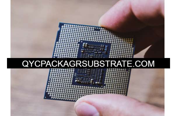
What is POP Package Substrate?
POP Package and POP Package Substrate Manufacturer. High speed and high frequency material packaging substrate manufacturing. Advanced packaging substrate production process and technology
POP stands for “Package on Package.” It’s a type of packaging technology used in semiconductor manufacturing, particularly in the production of integrated circuits (ICs) such as microprocessors and memory chips.
In a POP configuration, multiple ICs are stacked vertically on top of each other within a single package, with the top IC (the “daughter” package) mounted on top of the bottom IC (the “mother” package). This allows for increased functionality and performance in a smaller footprint, as well as improved electrical performance due to shorter interconnect lengths between the stacked ICs.
The substrate refers to the material layer that provides mechanical support and electrical connections between the stacked ICs within the package. It’s typically made of a material like organic laminate, silicon, or glass, and contains metal traces (wires) that connect the pins of the top IC to the underlying package and, ultimately, to the external circuitry.
POP packaging is commonly used in applications where space constraints are critical, such as in mobile devices like smartphones and tablets, where manufacturers aim to pack as much functionality as possible into a compact form factor.
POP Package Substrate
What are the functions of POP Package Substrate?
The POP package substrate serves several important functions in the overall operation and performance of integrated circuits (ICs) configured in a Package on Package (POP) arrangement. Here are some of its key functions:
Mechanical Support: The substrate provides structural support for the stacked ICs within the package, holding them securely in place and protecting them from physical damage during handling, assembly, and operation.
Electrical Interconnection: The substrate contains a network of metal traces (often made of copper) that provide electrical connections between the pins or pads of the top IC (daughter package) and the bottom IC (mother package), as well as to the external circuitry. These connections enable the transmission of signals, power, and data between the stacked ICs and the rest of the system.
Signal Routing: The substrate routes signals from the input/output (I/O) pads of the top IC to the appropriate pads or pins of the bottom IC and vice versa. This routing is carefully designed to minimize signal degradation and interference, ensuring reliable communication between the stacked ICs.
Power Distribution: The substrate distributes power from the power supply to the various components within the stacked ICs, ensuring that they receive the necessary voltage and current for proper operation. This may involve incorporating power distribution networks (such as power planes or power buses) into the substrate design.
Heat Dissipation: In some cases, the substrate may also play a role in dissipating heat generated by the stacked ICs during operation. This can be achieved through the use of thermally conductive materials or structures within the substrate, which help to conduct heat away from the ICs and dissipate it into the surrounding environment.
Overall, the POP package substrate is a critical component that facilitates the integration, electrical connectivity, and mechanical stability of stacked ICs within a compact package, enabling the realization of advanced electronic devices with enhanced functionality and performance.
What are the different types of POP Package Substrate?
There are several types of POP package substrates, each with its own characteristics and suitability for different applications. Some common types include:
Organic Substrate: Organic substrates, also known as organic laminate substrates, are made of materials such as epoxy resin or fiberglass reinforced with epoxy. They are widely used in POP packaging due to their low cost, lightweight, and good electrical properties. Organic substrates are suitable for applications where cost-effectiveness and moderate performance are prioritized.
Silicon Substrate: Silicon substrates are made of silicon material and are often used in high-performance POP applications, especially those requiring high-speed data transmission and low electrical resistance. Silicon substrates offer excellent electrical properties, thermal conductivity, and dimensional stability, making them ideal for demanding applications such as high-speed processors and memory modules.
Glass Substrate: Glass substrates are made of glass material and offer excellent dimensional stability, thermal properties, and high electrical insulation. They are commonly used in POP packaging for applications requiring high reliability and precision, such as medical devices, automotive electronics, and aerospace systems.
Ceramic Substrate: Ceramic substrates, typically made of alumina (aluminum oxide) or aluminum nitride, offer superior thermal conductivity, mechanical strength, and electrical insulation compared to organic substrates. They are often used in POP packaging for high-power applications and environments with extreme temperature variations, such as power amplifiers, RF modules, and LED drivers.
Metal Substrate: Metal substrates, such as copper or aluminum, are used in POP packaging for applications requiring high thermal conductivity and heat dissipation. They provide efficient thermal management by dissipating heat away from the stacked ICs, making them suitable for power electronics, LED lighting, and other high-power applications.
These are some of the main types of POP package substrates, each offering different properties and performance characteristics to meet the diverse requirements of various electronic devices and applications. The choice of substrate type depends on factors such as cost, performance, reliability, and thermal management requirements.
What is the relationship between POP Package Substrate and IC packaging?
The relationship between POP (Package on Package) package substrate and IC (Integrated Circuit) packaging is a close one, as POP is a specific type of IC packaging technology.
IC packaging involves the encapsulation of semiconductor chips (ICs) in protective housings or packages, providing mechanical support, electrical connections, and environmental protection. These packages serve to connect the ICs to external circuitry, facilitate heat dissipation, and ensure reliability in various operating conditions.
POP, on the other hand, is a packaging configuration where multiple IC packages are vertically stacked on top of each other within a single package. This stacking arrangement allows for increased functionality and performance in a smaller footprint, enabling the integration of multiple chips into a compact module.
The POP package substrate plays a crucial role in this configuration by providing mechanical support and electrical interconnection between the stacked ICs. It serves as the foundation upon which the IC packages are mounted and facilitates the transmission of signals, power, and data between the stacked layers. Additionally, the substrate may also contribute to thermal management by dissipating heat away from the ICs.
In summary, POP package substrate is a key component of IC packaging, particularly in the context of stacked configurations, enabling the realization of advanced electronic devices with enhanced functionality, performance, and miniaturization.
How does POP Package Substrate differ from PCB?
POP package substrate and PCB (Printed Circuit Board) are both essential components in electronic systems, but they serve different purposes and have distinct characteristics. Here’s how they differ:
Functionality:
POP Package Substrate: The primary function of a POP package substrate is to provide mechanical support and electrical interconnection between stacked integrated circuit (IC) packages within a single package. It facilitates the vertical stacking of ICs, allowing for increased functionality and performance in a compact form factor.
PCB: PCBs serve as the backbone of electronic systems, providing a platform for mounting and interconnecting various electronic components, including ICs, resistors, capacitors, and connectors. PCBs enable the routing of signals and power between components, forming the basis for electronic circuits.
Construction:
POP Package Substrate: POP package substrates are typically constructed using specialized materials optimized for high-density interconnects and thermal management. They may incorporate multiple layers of metal traces, vias, and insulating materials to facilitate the required electrical and mechanical properties for stacking IC packages.
PCB: PCBs are typically constructed using laminates made of fiberglass reinforced with epoxy resin (FR-4) or other substrate materials. They consist of multiple layers of conductive traces (copper) and insulating layers (dielectric) interconnected through vias. PCBs may also include components mounted on the surface or embedded within the substrate.
Application:
POP Package Substrate: POP package substrates are primarily used in applications requiring high integration density and miniaturization, such as mobile devices (smartphones, tablets), wearable electronics, and IoT (Internet of Things) devices.
PCB: PCBs are used in a wide range of electronic devices and systems, including computers, consumer electronics, industrial equipment, automotive electronics, and telecommunications equipment.
Interconnect Density:
POP Package Substrate: POP package substrates are designed to accommodate high-density interconnects between stacked IC packages, often utilizing advanced packaging technologies such as flip-chip bonding and fine-pitch wire bonding.
PCB: PCBs may vary in interconnect density depending on the application and design requirements. They can support various interconnect technologies, including through-hole vias, surface-mount pads, and ball grid arrays (BGAs).
In summary, while both POP package substrates and PCBs are integral to electronic systems, they serve different functions and are optimized for different applications and design considerations. POP package substrates focus on enabling the stacking of IC packages for increased integration density, while PCBs provide a platform for interconnecting electronic components in a wide range of electronic devices and systems.
What are the structure and production technology of POP Package Substrate?
The structure and production technology of POP (Package on Package) package substrates can vary depending on factors such as the specific application, performance requirements, and manufacturing capabilities of the semiconductor industry. However, I can provide an overview of the general structure and production process typically used for POP package substrates:
Structure:
Base Material: The substrate starts with a base material, which can vary depending on the desired properties such as thermal conductivity, electrical insulation, and mechanical strength. Common base materials include organic laminate (e.g., FR-4), silicon, glass, ceramic, or metal.
Layer Stackup: Multiple layers are typically used to construct the substrate. These layers may include conductive metal traces, insulating layers, and possibly additional features such as embedded passive components (e.g., resistors, capacitors), thermal management structures, and signal conditioning circuitry.
Interconnects: Metal traces are patterned on the substrate layers to provide electrical connections between the stacked IC packages and external circuitry. These traces may be fabricated using techniques such as lithography, thin-film deposition, and etching.
Vias: Vias are small holes drilled or etched through the substrate layers to provide vertical electrical connections between different layers. These vias can be filled with conductive material (e.g., copper) to ensure reliable electrical continuity.
Solder Mask: A solder mask layer is applied to the substrate to define the areas where solder joints will be formed during assembly. This helps to prevent solder bridging and ensure proper alignment of the IC packages.
Production Technology:
Design and Layout: The substrate design begins with the definition of electrical and mechanical requirements, as well as the layout of interconnects, vias, and other features. Computer-aided design (CAD) tools are commonly used to create and optimize the substrate layout.
Manufacturing Processes: The fabrication of POP package substrates involves a combination of semiconductor manufacturing processes, such as lithography, thin-film deposition, etching, drilling, and plating. These processes are used to create the desired patterns, features, and interconnects on the substrate layers.
Assembly: Once the substrate is fabricated, it undergoes assembly processes to attach the IC packages, typically using techniques such as flip-chip bonding, wire bonding, or solder ball attachment. The substrate may also include alignment and registration features to ensure accurate positioning of the stacked IC packages.
Testing and Quality Control: After assembly, the POP package substrates undergo testing to verify electrical functionality, interconnect integrity, and mechanical reliability. This may include electrical continuity testing, signal integrity analysis, thermal testing, and mechanical stress testing.
Overall, the production technology of POP package substrates involves a combination of advanced semiconductor manufacturing processes and assembly techniques to achieve the desired electrical and mechanical performance required for stacking IC packages in compact electronic devices.
Frequently Asked Questions (FAQs)
What is a POP package substrate?
A POP package substrate is a component used in semiconductor manufacturing that facilitates the stacking of integrated circuit (IC) packages within a single package. It provides mechanical support and electrical interconnection between the stacked IC packages.
What are the benefits of using POP package substrates?
POP package substrates enable increased functionality and performance in a smaller footprint, allowing for the integration of multiple ICs into compact electronic devices. They also help improve electrical performance by reducing interconnect lengths and enhancing thermal management.
What materials are used in POP package substrates?
POP package substrates can be made from various materials, including organic laminate (e.g., FR-4), silicon, glass, ceramic, and metal. The choice of material depends on factors such as cost, performance requirements, and thermal management considerations.
How are POP package substrates manufactured?
The manufacturing process for POP package substrates involves a combination of semiconductor manufacturing processes, such as lithography, thin-film deposition, etching, drilling, and plating. These processes are used to create the desired patterns, features, and interconnects on the substrate layers.
What are some applications of POP package substrates?
POP package substrates are commonly used in applications requiring high integration density and miniaturization, such as mobile devices (smartphones, tablets), wearable electronics, IoT (Internet of Things) devices, and other compact electronic devices.
How do POP package substrates differ from PCBs?
POP package substrates focus on facilitating the stacking of IC packages within a single package, whereas PCBs serve as the platform for interconnecting various electronic components in electronic systems. POP package substrates are optimized for high-density interconnects and thermal management in stacked configurations, while PCBs are more versatile and widely used in a variety of electronic devices and systems.
Conclusion
In conclusion, POP (Package on Package) package substrates play a crucial role in semiconductor manufacturing, particularly in the production of compact electronic devices requiring high integration density and performance. These substrates enable the stacking of multiple integrated circuit (IC) packages within a single package, providing mechanical support and electrical interconnection between the stacked ICs.
POP package substrates are constructed using specialized materials and manufacturing processes optimized for high-density interconnects, thermal management, and reliability. They can be made from various materials such as organic laminate, silicon, glass, ceramic, and metal, depending on the specific requirements of the application.
The production technology of POP package substrates involves a combination of semiconductor manufacturing processes, including lithography, thin-film deposition, etching, drilling, and plating. These processes are used to create the desired patterns, features, and interconnects on the substrate layers.
Overall, POP package substrates enable the realization of advanced electronic devices with enhanced functionality, performance, and miniaturization. They find applications in a wide range of industries, including mobile devices, wearable electronics, IoT devices, and other compact electronic devices.
As semiconductor technology continues to advance, the importance of POP package substrates is expected to grow, driving innovation in packaging design, materials, and manufacturing processes to meet the evolving demands of the electronics industry.