
What is QFN Package?
QFN Package service and Package substrate Manufacturer. We use advanced Msap and Sap technology, High multilayer interconnection substrates from 2 to 20 layers, We also offer the QFN Package and other types Package service.
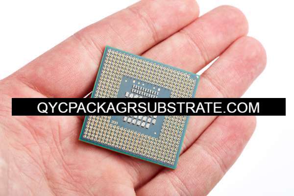
QFN stands for Quad Flat No-Lead package. It’s a type of surface-mount integrated circuit package. QFN packages are commonly used in modern electronics due to their compact size, excellent thermal and electrical performance, and ease of manufacturing.
Key features of QFN packages include:
No Leads: QFN packages have no leads protruding from the package, which allows for a very compact footprint on the circuit board.
Flat Contacts: The electrical connections are made via a series of flat contacts on the bottom of the package. These contacts are usually arranged in a grid pattern, hence the name “Quad Flat”.
Thermal Pad: Many QFN packages have a large thermal pad on the bottom, which helps dissipate heat away from the integrated circuit, improving thermal performance.
Exposed Die Pad: In some designs, the die pad (the area where the actual integrated circuit is located) is exposed on the bottom of the package, allowing for direct thermal contact with the circuit board.
Variety of Sizes: QFN packages come in various sizes and configurations, allowing designers to choose the most appropriate package for their specific application.
Overall, QFN packages offer a good balance of size, performance, and ease of use, making them popular choices for a wide range of electronic devices, including smartphones, tablets, and other consumer electronics, as well as industrial and automotive applications.
QFN Package
What are the functions of QFN Package?
The QFN (Quad Flat No-Lead) package serves several important functions in electronic devices:
Component Encapsulation: One of the primary functions of the QFN package is to encapsulate the integrated circuit (IC) or semiconductor device. It provides physical protection to the delicate semiconductor material from external elements such as moisture, dust, and mechanical stress.
Electrical Connection: The QFN package facilitates electrical connections between the integrated circuit and the external circuitry on the printed circuit board (PCB). The flat contacts or leads on the bottom of the package establish electrical connections with the PCB, enabling the flow of electrical signals and power to and from the IC.
Heat Dissipation: Many QFN packages incorporate a large thermal pad on the bottom of the package or expose the die pad directly. This feature helps dissipate heat generated by the integrated circuit during operation. Efficient heat dissipation is crucial for maintaining the performance and reliability of the IC, especially in high-power or high-frequency applications.
Space Efficiency: QFN packages offer a compact footprint on the PCB due to their flat, leadless design. This space-saving feature is particularly advantageous in applications where board space is limited or miniaturization is desired, such as in portable electronic devices like smartphones, tablets, and wearables.
Improved Electrical Performance: The absence of leads in QFN packages reduces parasitic inductance and capacitance, leading to improved electrical performance compared to traditional leaded packages. This can result in faster signal propagation, reduced electromagnetic interference (EMI), and improved high-frequency characteristics, making QFN packages suitable for a wide range of applications, including high-speed digital and RF (radio frequency) circuits.
Overall, QFN packages play a crucial role in modern electronics by providing a compact, reliable, and efficient solution for encapsulating and connecting integrated circuits while offering advantages in thermal management and electrical performance.
What are the different types of QFN Package?
There are several variations of the QFN (Quad Flat No-Lead) package, each designed to meet specific application requirements. Some common types of QFN packages include:
Thin QFN (TQFN): Thin QFN packages have a reduced profile compared to standard QFN packages, making them suitable for applications where height constraints are a concern, such as thin electronic devices like smartphones and tablets.
Micro QFN (µQFN): Micro QFN packages are even smaller than standard QFN packages, with a finer pitch and smaller overall dimensions. They are often used in miniaturized electronic devices and applications where space savings are critical.
Dual QFN (DQFN): Dual QFN packages feature two separate die pads within the same package, allowing for the integration of multiple integrated circuits or dies in a single package. This configuration can help reduce the overall footprint on the PCB and simplify assembly processes.
Power QFN (PQFN): Power QFN packages are designed to handle higher power dissipation requirements compared to standard QFN packages. They typically feature a larger thermal pad or additional thermal vias for improved heat dissipation, making them suitable for power electronics applications.
Exposed Pad QFN (EPQFN): Exposed pad QFN packages have the die pad exposed on the bottom of the package, allowing for direct thermal contact with the PCB. This configuration enhances thermal performance and is commonly used in high-power or high-temperature applications.
Leadframe QFN: Leadframe QFN packages incorporate a metal leadframe within the package structure, providing additional mechanical support and improved reliability compared to standard QFN packages. They are often used in automotive and industrial applications where robustness is essential.
Cavity QFN: Cavity QFN packages feature a recessed cavity within the package body, allowing for the integration of larger or stacked die configurations. This design enables higher levels of integration and functionality in a compact form factor.
These are just a few examples of the various types of QFN packages available in the market, each offering unique features and benefits tailored to specific application requirements. The choice of QFN package type depends on factors such as size constraints, thermal management needs, power dissipation requirements, and overall system design considerations.
What is the relationship between QFN Package and IC packaging?
The QFN (Quad Flat No-Lead) package is a type of integrated circuit (IC) packaging. IC packaging refers to the process of enclosing one or more semiconductor devices (integrated circuits or chips) in a protective casing or package. The package serves several important functions, including providing physical protection to the semiconductor die, establishing electrical connections with external circuitry, dissipating heat generated during operation, and enhancing the reliability and performance of the integrated circuit.
QFN packages are a specific category of IC packaging characterized by their flat, leadless design. They typically feature a square or rectangular body with metal contacts or leads arranged along the perimeter of the package’s bottom surface. QFN packages are widely used in modern electronics due to their compact size, excellent thermal and electrical performance, and ease of manufacturing.
The relationship between QFN packages and IC packaging is that QFN packages are a type of IC package used to encapsulate and connect semiconductor devices. They are designed to meet specific application requirements, such as space constraints, thermal management needs, and electrical performance criteria. QFN packages are just one of many types of IC packages available, with each type offering unique features and benefits suited to different applications and performance requirements.
How does QFN Package differ from PCB?
The QFN (Quad Flat No-Lead) package and PCB (Printed Circuit Board) are two distinct components used in electronic devices, each serving different functions and playing different roles in the overall system. Here’s how they differ:
Function:
QFN Package: The QFN package encapsulates and houses the integrated circuit (IC) or semiconductor device. It provides physical protection to the IC, establishes electrical connections with the PCB, and helps dissipate heat generated by the IC during operation.
PCB: The PCB provides a platform for mounting and interconnecting various electronic components, including ICs, resistors, capacitors, and connectors. It serves as the backbone of the electronic device, providing mechanical support and facilitating electrical connections between components.
Composition:
QFN Package: QFN packages are typically made of materials such as plastic, ceramic, or a combination of both. They feature a flat, leadless design with metal contacts or leads on the bottom surface for electrical connections.
PCB: PCBs are typically made of layers of fiberglass or other composite materials with conductive copper traces etched onto the surface. Components are soldered onto the PCB, and electrical connections are established through the traces and vias on the board.
Size and Shape:
QFN Package: QFN packages come in various sizes and shapes, including square, rectangular, and even custom shapes. They are designed to accommodate different IC sizes and configurations while minimizing the footprint on the PCB.
PCB: PCBs come in a wide range of sizes and shapes, depending on the specific application and design requirements. They can vary from small, compact boards used in handheld devices to large, multi-layer boards used in complex electronic systems.
Role in the System:
QFN Package: The QFN package primarily houses and protects the integrated circuit, providing electrical connections and thermal management capabilities. It directly interfaces with the PCB to facilitate the flow of electrical signals and power.
PCB: The PCB serves as the platform for assembling and interconnecting various electronic components to create a functional electronic system. It provides mechanical support, electrical connections, and a means for integrating and organizing components to achieve the desired functionality.
In summary, while both the QFN package and PCB are essential components in electronic devices, they serve different functions and have distinct characteristics. The QFN package encapsulates and protects the integrated circuit, while the PCB provides a platform for mounting components and establishing electrical connections to create a complete electronic system.
What are the structure and production technology of QFN Package?
The structure and production technology of QFN (Quad Flat No-Lead) packages involve several key steps and components. Here’s an overview of the typical structure and production process:
Structure:
QFN packages typically consist of the following components:
Die: The semiconductor die, which contains the integrated circuit (IC) or semiconductor device.
Package Body: The main body of the package, which encapsulates the die and provides physical protection. It is usually made of plastic, ceramic, or a combination of both.
Leadframe: A metal leadframe embedded within the package body, which provides structural support and electrical connections. The leadframe typically includes bond pads for wire bonding and metal contacts or leads for surface-mounting onto the PCB.
Thermal Pad: Some QFN packages feature a large thermal pad on the bottom of the package, which helps dissipate heat generated by the die during operation.
Production Technology:
Die Preparation: The semiconductor die is prepared by fabricating the integrated circuit on a silicon wafer through processes such as photolithography, etching, doping, and deposition.
Leadframe Fabrication: The leadframe is fabricated separately using metal stamping or etching techniques. It is designed to accommodate the specific dimensions and configuration of the die and package body.
Die Attach: The semiconductor die is attached to the center of the leadframe using a conductive adhesive or solder paste. This step ensures proper alignment and electrical connection between the die and the leadframe.
Wire Bonding: Thin wires (usually made of gold or aluminum) are bonded between the bond pads on the die and the corresponding pads on the leadframe. Wire bonding provides electrical connections between the die and the external contacts or leads.
Molding: The assembled die and leadframe are encapsulated within the package body using a molding compound (typically epoxy resin). The molding compound provides physical protection to the die and wire bonds and helps maintain the structural integrity of the package.
Lead Formation: If the QFN package has leads or contacts on the bottom surface, they are formed using techniques such as stamping, plating, or soldering.
Testing and Inspection: The completed QFN packages undergo various tests and inspections to ensure proper functionality, electrical performance, and reliability. This may include electrical testing, visual inspection, and thermal cycling tests.
Overall, the production of QFN packages involves a combination of semiconductor manufacturing processes (for die fabrication) and packaging assembly techniques (for leadframe fabrication, die attachment, wire bonding, encapsulation, and lead formation). These processes are carefully controlled to achieve high yields, consistent quality, and reliable performance in the final packaged devices.
Frequently Asked Questions (FAQs)
What does QFN stand for?
QFN stands for Quad Flat No-Lead. It’s a type of surface-mount integrated circuit package.
What are the advantages of QFN packages?
QFN packages offer several advantages, including compact size, excellent thermal and electrical performance, ease of manufacturing, and suitability for high-frequency applications.
What are the main components of a QFN package?
The main components of a QFN package include the semiconductor die, package body, leadframe, thermal pad (if present), and metal contacts or leads.
How are QFN packages manufactured?
The manufacturing process for QFN packages involves several steps, including die preparation, leadframe fabrication, die attach, wire bonding, encapsulation, lead formation, testing, and inspection.
What are the different types of QFN packages?
Common types of QFN packages include Thin QFN (TQFN), Micro QFN (µQFN), Dual QFN (DQFN), Power QFN (PQFN), Exposed Pad QFN (EPQFN), Leadframe QFN, and Cavity QFN, among others.
What are the applications of QFN packages?
QFN packages are used in a wide range of electronic devices and applications, including smartphones, tablets, consumer electronics, industrial equipment, automotive systems, and telecommunications devices.
How do QFN packages differ from other types of IC packages?
QFN packages differ from other IC packages in terms of their leadless design, compact size, thermal performance, and electrical characteristics. They are often compared to packages like SOP (Small Outline Package), QFP (Quad Flat Package), and BGA (Ball Grid Array).
What factors should be considered when selecting a QFN package for a specific application?
Factors to consider when selecting a QFN package include package size, lead pitch, thermal characteristics, electrical performance, reliability requirements, and compatibility with assembly processes.
What are some common failure modes of QFN packages?
Common failure modes of QFN packages include solder joint failure, wire bond failure, delamination, package cracking, and thermal issues such as overheating or insufficient heat dissipation.
How can I ensure proper soldering of QFN packages onto a PCB?
Proper soldering of QFN packages onto a PCB requires careful attention to solder paste deposition, accurate placement, appropriate reflow profile, and thorough inspection to ensure solder joint quality and reliability.
Conclusion
In conclusion, the QFN (Quad Flat No-Lead) package is a versatile and widely used type of integrated circuit (IC) package in modern electronics. Its compact size, excellent thermal and electrical performance, and ease of manufacturing make it suitable for a variety of applications, ranging from consumer electronics to industrial and automotive systems.
The structure of a QFN package typically includes a semiconductor die, package body, leadframe, and optional thermal pad or exposed die pad. The production technology involves various steps such as die preparation, leadframe fabrication, die attach, wire bonding, encapsulation, lead formation, testing, and inspection.
Frequently asked questions (FAQs) about QFN packages cover topics such as their advantages, components, manufacturing process, types, applications, differences from other IC packages, failure modes, and soldering considerations.
Overall, QFN packages play a crucial role in electronic device design and manufacturing, offering designers a compact, reliable, and efficient solution for encapsulating and connecting integrated circuits while providing advantages in thermal management and electrical performance.