
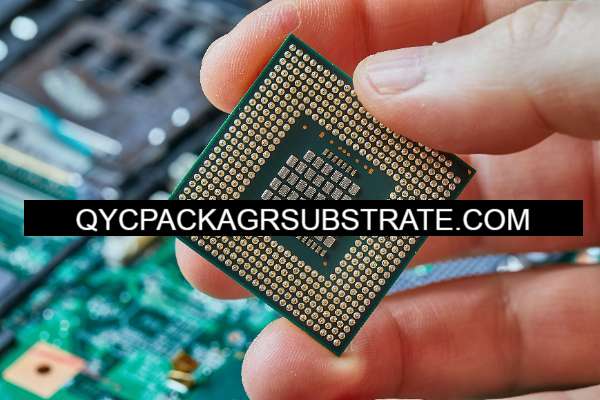
RF High Frequency Package Substrates Manufacturer
RF High Frequency Package Substrates Manufacturer,RF High Frequency Package Substrates are critical components designed to handle high-frequency signals, widely used in wireless communication, radar, and satellite communication. These substrates utilize high-quality high-frequency materials like PTFE (polytetrafluoroethylene), offering low dielectric loss and excellent signal transmission properties. They are designed with considerations for signal integrity and interference resistance, typically employing multilayer structures, precise impedance control, and effective shielding techniques. RF High Frequency Package Substrates minimize signal attenuation and crosstalk, ensuring stability and reliability in high-frequency environments, crucial for device performance.
What are RF High Frequency Package Substrates?
RF High Frequency Package Substrates are specialized materials used in the construction of electronic packages for high-frequency applications, typically above 1 GHz. These substrates are engineered to provide excellent electrical properties such as low dielectric constant (εr) and low loss tangent (tan δ), which are crucial for minimizing signal loss and maintaining signal integrity at high frequencies.
The substrates are often made from materials like PTFE (Polytetrafluoroethylene) or ceramic-filled PTFE composites, which offer superior electrical characteristics compared to traditional FR-4 substrates used in lower frequency applications. They are designed to support the transmission of high-frequency signals with minimal attenuation and distortion.
In addition to their electrical properties, RF High Frequency Package Substrates are also designed to have good thermal stability, mechanical strength, and reliability under various environmental conditions. They are commonly used in applications such as microwave circuits, radar systems, satellite communications, and wireless infrastructure where high performance and reliability are critical.
Manufacturers of RF High Frequency Package Substrates continually innovate to improve their materials, offering substrates with even lower εr, lower loss, and enhanced thermal management capabilities to meet the evolving demands of high-frequency electronics. These substrates play a crucial role in enabling the development of advanced RF and microwave devices that power modern communication and radar systems.
RF High Frequency Package Substrates Manufacturer
What are the RF High Frequency Package Substrates Design Guidelines?
Designing with RF High Frequency Package Substrates involves adhering to specific guidelines to ensure optimal performance in high-frequency applications. Here are some key design guidelines:
- Material Selection: Choose substrates with low dielectric constant (εr) and low loss tangent (tan δ). Common materials include PTFE (e.g., Teflon) and ceramic-filled PTFE composites. These materials minimize signal loss and maintain signal integrity at high frequencies.
- Layer Stackup: Design a layer stackup that minimizes electromagnetic interference (EMI) and cross-talk between adjacent signal traces. Maintain controlled impedance by specifying trace widths, thicknesses, and spacing according to the substrate material’s dielectric properties.
- Grounding: Ensure effective grounding to minimize noise and interference. Use solid ground planes and vias to connect ground layers effectively. Ground vias should be placed close to signal vias to reduce inductance and impedance.
- Transmission Line Design: Use transmission line structures (e.g., microstrips or coplanar waveguides) that are suitable for high-frequency signals. Maintain consistent impedance along transmission lines to prevent reflections and signal degradation.
- Component Placement: Place components strategically to minimize parasitic effects and optimize signal paths. Maintain adequate spacing between components to reduce mutual coupling and interference.
- Thermal Management: Consider thermal management techniques such as thermal vias and heat sinks to dissipate heat effectively, especially in high-power RF applications. Ensure substrate materials have adequate thermal conductivity.
- Manufacturability: Design with manufacturability in mind, considering the capabilities and limitations of fabrication processes (e.g., PCB manufacturing). Ensure that design specifications can be reliably translated into physical substrates.
- Simulation and Testing: Use electromagnetic simulation tools to verify design performance before fabrication. Perform signal integrity analysis, impedance matching, and electromagnetic interference (EMI) analysis to ensure compliance with design goals.
- Environmental Considerations: Design substrates to withstand environmental conditions relevant to the application (e.g., temperature, humidity, vibration). Ensure substrate materials have appropriate mechanical strength and reliability.
By following these design guidelines, engineers can effectively harness the capabilities of RF High Frequency Package Substrates to achieve high-performance, reliable electronic systems for applications demanding robust high-frequency operation.
What is the RF High Frequency Package Substrates Fabrication Process?
The fabrication process of RF High Frequency Package Substrates involves several specialized steps to ensure the materials meet stringent requirements for high-frequency applications. Here are the typical stages involved in their fabrication:
- Material Selection: The process begins with the selection of appropriate substrate materials. Common choices include PTFE (Polytetrafluoroethylene) and ceramic-filled PTFE composites due to their low dielectric constant (εr) and low loss tangent (tan δ), which are crucial for minimizing signal loss at high frequencies.
- Preparation of Substrate Materials: The selected substrate materials undergo preparation steps such as cutting or shearing to the desired dimensions. The surfaces are cleaned thoroughly to remove any contaminants that could affect subsequent processing steps.
- Layer Stacking and Lamination:If multiple layers are required (typical in multilayer PCBs), individual substrate layers are stacked according to the design specifications. The layers are then laminated together under controlled temperature and pressure conditions. Lamination ensures proper bonding between layers and forms a solid structure.
- Drilling: After lamination, precision drilling is performed to create holes for vias and component leads. The drilling process must maintain tight tolerances to ensure accurate alignment of vias and proper clearance for component mounting.
- Copper Plating: Copper foil is bonded to the substrate surfaces through an electroplating process. This step involves applying a thin layer of copper to the substrate to form conductive traces and pads. The thickness and quality of the copper plating are critical to achieving desired electrical performance.
- Circuit Patterning: Using photolithography or direct imaging techniques, a pattern of conductive traces and pads is defined on the copper-clad substrate. This step involves applying a photoresist layer, exposing it to UV light through a photomask, and developing it to selectively remove the photoresist and expose the copper for etching.
- Etching: Copper that is not protected by the developed photoresist is etched away using an etchant solution, leaving behind the desired circuit pattern on the substrate. Careful control of the etching process ensures that trace widths and spacing meet design specifications for controlled impedance.
- Surface Finish: Once the circuit pattern is defined, a surface finish is applied to the exposed copper to protect it from oxidation and facilitate soldering during assembly. Common surface finishes include immersion gold, immersion silver, and HASL (Hot Air Solder Leveling).
- Final Inspection and Testing: After fabrication, the substrates undergo rigorous inspection and testing to verify dimensional accuracy, electrical continuity, and adherence to design specifications. Testing may include electrical tests such as impedance measurements and insulation resistance tests.
- Quality Assurance: Throughout the fabrication process, stringent quality control measures are implemented to ensure consistency and reliability of the RF High Frequency Package Substrates. This includes monitoring process parameters, material characteristics, and final product performance.
By following these steps meticulously, manufacturers can produce RF High Frequency Package Substrates that meet the demanding requirements of high-frequency electronic applications, ensuring optimal signal integrity, reliability, and performance.
How do you manufacture RF High Frequency Package Substrates?
Manufacturing RF High Frequency Package Substrates involves a series of specialized processes designed to achieve precise electrical properties and performance suitable for high-frequency applications. Here’s a detailed outline of the manufacturing process:
- Material Selection: Begin by selecting substrate materials with low dielectric constant (εr) and low loss tangent (tan δ), such as PTFE (Polytetrafluoroethylene) or ceramic-filled PTFE composites. These materials provide excellent electrical characteristics necessary for minimizing signal loss at high frequencies.
- Substrate Preparation:Prepare the substrate materials by cutting or shearing them to the required dimensions. Clean the substrate surfaces thoroughly to remove contaminants that could impact subsequent processing steps.
- Layer Stacking and Lamination: If producing multilayer substrates, stack individual layers according to the design specifications. Use laminating presses to bond the layers together under controlled temperature and pressure conditions. This ensures strong adhesion between layers and forms a solid substrate structure.
- Drilling: After lamination, precision drilling is performed to create holes for vias and component leads. The drilling process must maintain tight tolerances to ensure accurate alignment of vias and proper clearance for component mounting.
- Copper Foil Bonding: Apply copper foil to both sides of the substrate through an electroplating process. This step involves depositing a thin layer of copper onto the substrate surfaces to form conductive traces and pads.
- Circuit Patterning: Define the circuit pattern on the copper-clad substrate using photolithography or direct imaging techniques. Apply a photoresist layer, expose it to UV light through a photomask, and develop it to selectively remove the photoresist, exposing the copper for etching.
- Etching: Use an etchant solution to remove the exposed copper, leaving behind the desired circuit pattern. Control the etching process carefully to achieve precise trace widths and spacing, crucial for maintaining controlled impedance.
- Surface Finish Application: Apply a surface finish to the exposed copper traces and pads to protect them from oxidation and facilitate soldering during assembly. Common surface finishes include immersion gold, immersion silver, and HASL (Hot Air Solder Leveling).
- Final Inspection and Testing: Conduct thorough inspection and testing of the manufactured substrates to ensure they meet dimensional accuracy, electrical continuity, and adherence to design specifications. Perform electrical tests such as impedance measurements and insulation resistance tests to verify performance.
- Packaging and Shipping: Once substrates pass quality assurance checks, package them securely to protect against damage during transit. Ensure proper labeling and documentation for traceability.
Throughout the manufacturing process, maintain stringent quality control measures to ensure consistency and reliability of RF High Frequency Package Substrates. Continuous monitoring of process parameters and material characteristics helps achieve high-quality substrates that meet the demanding requirements of high-frequency electronic applications.
How much should RF High Frequency Package Substrates cost?
Manufacturing RF High Frequency Package Substrates involves a series of precise steps and specialized processes tailored to meet the stringent requirements of high-frequency electronic applications:
- Material Selection: Choose substrate materials with low dielectric constant (εr) and low loss tangent (tan δ), such as PTFE (Polytetrafluoroethylene) or ceramic-filled PTFE composites. These materials are selected for their excellent electrical properties, crucial for minimizing signal loss at high frequencies.
- Preparation of Substrate Materials: Begin by preparing the substrate materials to the required dimensions. This typically involves cutting or shearing large sheets of substrate material to size. The surfaces are meticulously cleaned to remove any contaminants that could affect subsequent processing steps.
- Layer Stacking and Lamination: If manufacturing multilayer substrates, stack the prepared substrate layers according to the design requirements. The layers are then laminated together under controlled temperature and pressure conditions to ensure proper bonding and the formation of a solid substrate structure.
- Drilling: Precision drilling is performed to create holes for vias and component leads. This step requires high accuracy to ensure proper alignment of vias between layers and adequate clearance for component mounting.
- Copper Cladding:Bond copper foil to the substrate surfaces through an electroplating process. This copper cladding forms the conductive traces and pads necessary for circuitry. The thickness and quality of the copper cladding are critical for achieving desired electrical performance.
- Circuit Patterning: Define the circuit pattern on the substrate using photolithography or direct imaging techniques. A photoresist layer is applied and exposed to UV light through a photomask, then developed to selectively remove the resist and expose the copper for etching.
- Etching: Etch away the unprotected copper using an etchant solution, leaving behind the desired circuit pattern. Etching must be controlled precisely to achieve accurate trace widths and spacing, ensuring controlled impedance for high-frequency signals.
- Surface Finish: Apply a surface finish to protect exposed copper and facilitate soldering during assembly. Common surface finishes include immersion gold, immersion silver, and HASL (Hot Air Solder Leveling).
- Final Inspection and Testing: Conduct thorough inspection and testing of the manufactured substrates to ensure they meet dimensional specifications and electrical performance requirements. Tests may include impedance measurements, insulation resistance tests, and visual inspection for defects.
- Packaging and Shipping: Once substrates pass quality assurance checks, package them securely for shipment to customers or assembly facilities. Proper packaging ensures protection from physical damage and environmental contaminants.
Throughout the manufacturing process, strict quality control measures are implemented to maintain consistency and reliability of RF High Frequency Package Substrates. Continuous monitoring of process parameters and material characteristics ensures that substrates meet the demanding standards of high-frequency applications, supporting optimal signal integrity and performance in electronic systems.
What is RF High Frequency Package Substrates base material?
RF High Frequency Package Substrates typically use specialized base materials that provide excellent electrical properties suited for high-frequency applications. The primary base materials include:
- PTFE (Polytetrafluoroethylene): PTFE is widely used due to its extremely low dielectric constant (εr) and low loss tangent (tan δ), which minimize signal loss and maintain signal integrity at high frequencies. PTFE substrates are often reinforced with glass fibers or ceramic fillers to enhance mechanical strength and dimensional stability.
- Ceramic-filled PTFE Composites: These composites combine the low εr and low tan δ properties of PTFE with the added benefits of high thermal conductivity and mechanical strength provided by ceramic fillers (such as alumina or silica). Ceramic-filled PTFE substrates are ideal for applications requiring excellent thermal management and robust mechanical performance alongside high-frequency operation.
These base materials are chosen for their ability to support the transmission of high-frequency signals with minimal attenuation and distortion. They also exhibit good thermal stability, chemical resistance, and reliability under various environmental conditions, making them suitable for critical applications in RF and microwave systems.
Manufacturers continually innovate and refine these base materials to achieve even lower dielectric constants, lower loss tangents, and improved thermal properties, thereby pushing the boundaries of performance in high-frequency electronic packaging.
Which company makes RF High Frequency Package Substrates?
RF high-frequency package substrates are typically manufactured by several specialized companies that provide various materials and technological solutions suitable for high-frequency electronic applications. Some well-known companies include Rogers Corporation in the United States, Mitsubishi Electric in Japan, Evonik’s ROHACELL in Germany, as well as several Chinese manufacturers like Aerospace Yunhai and China WBT.
As for our company, we have the capability and experience to produce RF high-frequency package substrates, focusing on electronic materials and high-frequency electronic packaging solutions. Here are the key capabilities and strengths we offer:
- Material Selection and R&D: We extensively research and master a variety of high-performance substrate materials, particularly those with low dielectric constant and low loss tangent, such as PTFE and ceramic-filled PTFE composites. We collaborate closely with material suppliers to ensure the selection and use of materials that best suit specific applications.
- Process Technology and Manufacturing Capability: We possess advanced process technology and manufacturing capabilities to perform critical processes such as multilayer substrate stacking, lamination, drilling, copper foil cladding, circuit pattern definition (including photolithography and direct imaging), etching, and surface finishing. Our production facilities are equipped with state-of-the-art equipment and automated production lines, ensuring high efficiency and quality.
- Quality Control and Certification: We strictly adhere to international standards and customer requirements, implementing comprehensive quality control measures. Our products undergo rigorous inspection and testing, including electrical performance tests (such as impedance measurements), mechanical performance tests, and environmental suitability tests, ensuring reliability and stability in various application environments.
- Customization and Technical Support: We value close collaboration with customers and can customize designs and produce high-performance RF high-frequency package substrates based on specific customer requirements. Our professional technical team and engineers provide comprehensive technical support and solution services, assisting customers in achieving their design goals and market demands.
In summary, our company is dedicated to providing high-performance and highly reliable RF high-frequency package substrate solutions with our expertise in technology, advanced manufacturing capabilities, and rigorous quality management system. We strive to innovate and advance in the field of electronic materials, contributing our efforts and knowledge to the global high-frequency electronic market.
What are the 7 qualities of good customer service?
Good customer service is characterized by several key qualities that contribute to positive customer experiences and satisfaction. Here are seven qualities that define good customer service:
- Responsiveness: Good customer service involves promptly addressing customer inquiries, concerns, and requests. Customers appreciate quick responses that demonstrate attentiveness to their needs.
- Empathy: Showing empathy means understanding and acknowledging the customer’s feelings and perspectives. Empathetic responses demonstrate that you care about the customer’s experience and are willing to help.
- Clear Communication: Effective communication is essential in customer service. It involves clearly conveying information, instructions, and solutions in a manner that is easy for the customer to understand.
- Product Knowledge: Good customer service representatives possess comprehensive knowledge about the products or services they support. This allows them to provide accurate information, answer questions, and offer relevant recommendations.
- Problem-Solving Skills: Customers often seek assistance with challenges or issues they encounter. Strong problem-solving skills enable customer service representatives to identify root causes, propose solutions, and resolve issues effectively.
- Professionalism: Maintaining professionalism in all interactions with customers is crucial. This includes being courteous, respectful, and maintaining a positive attitude, even in challenging situations.
- Follow-up and Follow-through: After addressing a customer’s concern or request, good customer service involves following up to ensure the issue is fully resolved and the customer is satisfied. Follow-through also includes keeping promises and commitments made to the customer.
By embodying these qualities, organizations can build trust, foster loyalty, and create positive relationships with their customers, ultimately leading to improved customer retention and business success.
FAQs
What are RF High Frequency Package Substrates?
RF High Frequency Package Substrates are specialized materials used in electronic packaging for high-frequency applications, typically above 1 GHz. They are designed to minimize signal loss and maintain signal integrity at these frequencies.
What materials are used for RF High Frequency Package Substrates?
Common materials include PTFE (Polytetrafluoroethylene) and ceramic-filled PTFE composites. These materials have low dielectric constants and low loss tangents, which are essential for high-frequency performance.
What are the key benefits of using RF High Frequency Package Substrates?
RF High Frequency Package Substrates offer benefits such as low signal loss, excellent high-frequency performance, good thermal stability, and reliability in various environmental conditions. They are crucial for applications like microwave circuits, radar systems, and wireless communication.
How do RF High Frequency Package Substrates differ from standard PCB materials?
RF substrates are optimized for high-frequency operation with lower dielectric constants and loss tangents compared to standard PCB materials like FR-4. This ensures minimal signal attenuation and distortion at higher frequencies.
What factors should be considered when selecting RF High Frequency Package Substrates?
Factors include dielectric constant (εr), loss tangent (tan δ), thermal conductivity, mechanical strength, dimensional stability, and compatibility with manufacturing processes such as drilling, etching, and plating.
What are typical applications of RF High Frequency Package Substrates?
They are used in microwave circuits, RF amplifiers, antennas, satellite communication systems, radar systems, wireless infrastructure, and other high-frequency electronic devices where signal integrity and performance are critical.
How are RF High Frequency Package Substrates manufactured?
Manufacturing involves processes such as material preparation, layer stacking, lamination, drilling, copper plating, circuit patterning (photolithography or direct imaging), etching, surface finishing, and rigorous quality testing to ensure performance specifications are met.