
Semiconductor BGA Substrate Manufacturer and package substrate manufacturer. We use advanced Msap and Sap technology, High multilayer interconnection substrates from 2 to 20 layers.
The Semiconductor BGA Substrate assumes a crucial role in the packaging of integrated circuits (ICs), with a specialized focus on Ball Grid Array (BGA) packages. Its significance lies in acting as a vital conduit that connects the IC—whether it’s a microprocessor or a graphics processing unit—to the printed circuit board (PCB) within electronic devices. This particular component is fundamental for the establishment and facilitation of essential connections between the IC and the PCB.
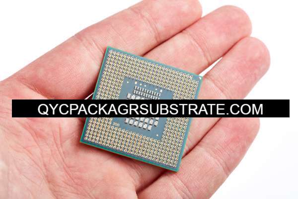
The BGA package features a grid of solder balls on its underside, establishing electrical connections between the IC and the PCB. This is where the BGA substrate comes into play – a thin, flat layer housing a network of conductive traces and vias. These elements facilitate the efficient routing of signals between the IC die and the solder balls.
In essence, the BGA substrate is fundamental for ensuring optimal electrical performance, effective thermal management, and durable mechanical reliability of the semiconductor package. Typically composed of layers of copper and insulating materials, the substrate material takes the form of a laminate.
The widespread use of BGA substrates has significantly risen in contemporary electronic devices, driven by their benefits in terms of compact space utilization, signal integrity improvement, and efficient heat dissipation. With the continuous advancement of electronic technology, the precise design and manufacturing of BGA substrates continue to be crucial in addressing the increasing requirements for improved performance, reduced size, and overall reliability in semiconductor packaging.
How Does Semiconductor BGA Substrate Function?
Semiconductor Ball Grid Array (BGA) substrates hold a central position in the architecture of electronic devices, serving as the foundational element for the integration of integrated circuits (ICs) and the establishment of vital interconnections between the IC and the Printed Circuit Board (PCB).The nuanced functions of BGA substrates contribute significantly to the overall efficacy of electronic systems.
Primarily, these substrates offer a stable and secure platform for the attachment of ICs, ensuring proper alignment and providing robust physical support within the packaging.
Moreover, BGA substrates act as a vital electrical interface between the IC and the PCB. Incorporating a network of conductive traces and vias, they form pathways for efficient signal transmission between the IC and the solder balls arranged in a grid on the underside of the package. This grid establishes essential electrical connections with the PCB.
Additionally, BGA substrates actively contribute to proficient heat dissipation.The compact design of Semiconductor Ball Grid Array (BGA) substrates is instrumental in accommodating a higher pin count within confined spaces, leading to an improvement in thermal conductivity. This becomes particularly critical in high-performance electronic devices, as it serves to prevent overheating and guarantees the reliability and longevity of semiconductor components through effective thermal management.
In summary, Semiconductor BGA Substrates play a pivotal role in electronic device functionality, providing a stable mounting platform, facilitating essential electrical connections, and aiding in efficient heat dissipation. These collective functions enhance the efficiency, reliability, and overall performance of advanced electronic systems.
What Functions Does Semiconductor BGA Substrate Fulfill?
Semiconductor Ball Grid Array (BGA) substrates perform a wide range of essential functions vital for the effective operation of electronic devices:
Sturdy Foundation: BGA substrates serve as a stable and secure base for affixing integrated circuits (ICs), ensuring precise alignment and robust support within the device’s packaging.
Electrical Connectivity: Functioning as a crucial electrical interface between the IC and the Printed Circuit Board (PCB), BGA substrates feature a network of conductive traces and vias. This configuration facilitates efficient electrical signal transmission, enhancing overall signal integrity.
Space-Efficient Design: With their compact design, BGA substrates enable a higher pin count within constrained spaces, supporting initiatives in device miniaturization and allowing for the creation of compact electronic devices.
Efficient Thermal Regulation: BGA substrates play a pivotal role in effectively managing heat. The compact design enhances thermal conductivity, creating an efficient pathway for the dissipation of heat from semiconductor components. This functionality is particularly critical in averting overheating, especially in high-performance applications.
Enhanced Device Reliability: Through active participation in thermal management, BGA substrates contribute to preventing overheating, thereby elevating the overall reliability and endurance of semiconductor components.
Optimized Signal Transmission: BGA substrates contribute to superior electrical performance by optimizing signal transmission. The shortened connection paths between the semiconductor device and the PCB reduce the risk of electrical noise, ensuring seamless and efficient high-speed data transfer.
In summary, Semiconductor BGA Substrates play a diverse and integral role in electronic devices, providing a stable foundation, facilitating vital electrical connections, optimizing heat dissipation, and contributing to the overall reliability and performance of advanced electronic systems.
What Are the Different Types of Semiconductor BGA Substrate?
Semiconductor Ball Grid Array (BGA) substrates come in diverse types, each tailored to specific materials, designs, and applications to meet the varied needs of electronic devices.
Material Variety: These substrates are commonly constructed from laminate composites, integrating layers of copper and insulating materials. This composition strikes a balance between electrical conductivity and insulation.
Design Variances: BGA substrates exhibit variations in design, including differences in layer count, conductive trace layouts, and solder ball arrangements. These design nuances cater to specific requirements such as signal integrity, thermal management, and overall performance.
Application-Specific: The selection of a BGA substrate type is often driven by the intended application. High-performance computing devices may prioritize substrates with advanced thermal dissipation capabilities, while those in consumer electronics may lean towards compact designs for space efficiency.
In addition to substrate types, BGA technology encompasses classifications of chip package technologies:
Flip-Chip BGA (FCBGA): This cutting-edge approach involves directly flipping and mounting the IC chip onto the substrate. By reducing interconnection paths, FCBGA enhances heat dissipation, making it a preferred choice for optimizing overall performance efficiently.
Ceramic BGA (CBGA): CBGA utilizes a ceramic substrate, providing superior thermal conductivity and reliability. This option is particularly well-suited for applications that demand robustness and resilience in challenging environmental conditions.
Organic BGA (OBGA): OBGA utilizes organic substrates, typically fiberglass-reinforced epoxy resins. Recognized for their lightweight and cost-effective design, OBGA is widely employed in a diverse range of consumer electronics, balancing performance and affordability.
Metal Core BGA (MCBGA): MCBGA distinguishes itself with a metal core substrate, often crafted from aluminum or copper. This design significantly improves thermal performance, making it a top choice for applications where efficient heat dissipation is crucial for sustained functionality.
In summary, Semiconductor BGA Substrates exhibit a range of materials, designs, and applications. Understanding the distinctions in chip package technologies associated with these substrates is crucial for selecting the most fitting option based on specific electronic device requirements.
How Does Semiconductor BGA Substrate Differ from Traditional PCBs?
Semiconductor Ball Grid Array (BGA) Substrates distinguish themselves from traditional Printed Circuit Boards (PCBs) through unique design, materials, and functionality. These differences set BGA substrates apart when juxtaposed with PCBs, Printed Wiring Boards (PWBs), motherboards, and related technologies.
Package Design:
Traditional PCBs: Typically feature flat designs with surface-mounted components.
Semiconductor BGA Substrates: Adopt a Ball Grid Array packaging design, directly mounting the IC chip onto the substrate. This configuration enhances heat dissipation and streamlines interconnection paths.
Materials:
Traditional PCBs: Often use materials like FR-4 for cost-effectiveness.
Semiconductor BGA Substrates: Employ specialized materials such as ceramics or organic substrates. These choices cater to high-density packaging and thermal management requirements.
Interconnection Paths:
Traditional PCBs: Involve intricate interconnection paths between components.
Semiconductor BGA Substrates: Leverage the BGA design to simplify interconnections, improving signal integrity and minimizing the risk of signal loss.
Thermal Management:
Traditional PCBs: May encounter challenges in efficiently dissipating heat.
Semiconductor BGA Substrates: Integrate efficient thermal management mechanisms, vital for applications with substantial heat generation. This ensures optimal performance and reliability.
Applications:
Traditional PCBs: Commonly deployed in various electronic devices with diverse applications.
Semiconductor BGA Substrates: Specifically tailored for semiconductor devices and high-performance applications where compact form factors and effective heat dissipation are crucial.
What Constitutes the Structure and Production Technologies of Semiconductor BGA Substrate?
Semiconductor Ball Grid Array (BGA) Substrates exhibit an intricate internal structure and employ cutting-edge production technologies for superior performance. The internal design includes dedicated layers for signal transmission, power distribution, and specialized functions, interconnected through vias to ensure efficiency.
In terms of production, two key methodologies contribute to the advanced capabilities of these substrates:
Improved High-Density Interconnect (HDI) Fabrication:
Microvia Technology: Utilizing micro-sized vias for enhanced routing density and improved signal integrity.
Sequential Build-Up (SBU) Process: Constructing layers incrementally to incorporate finer traces and smaller vias, boosting overall density.
Semi-Additive Methods:
Laser Direct Imaging (LDI):Utilizing precise laser technology for the direct transfer of circuit patterns onto the substrate ensures unparalleled accuracy while minimizing material wastage.
Copper Pillar Technology: Enhancing electrical performance and reliability, semiconductor chips are directly affixed to the substrate through the utilization of copper pillars.
These advanced production techniques effectively address challenges related to miniaturization, signal integrity, and thermal management. The collaboration of Improved HDI fabrication and semi-additive methods results in Semiconductor BGA Substrates with finer features, tighter interconnections, and superior functionality, meeting the stringent requirements of modern high-performance semiconductor applications.
What Are Common Questions About Semiconductor BGA Substrates?
How Does BGA Substrate Differ from Traditional PCBs?
BGA Substrates differ by design and materials, utilizing specialized substances like ceramics. The BGA design involves direct mounting of the IC chip, streamlining interconnections and enhancing thermal performance.
What Are the Key Components of BGA Substrates?
BGA Substrates consist of signal layers for electrical transmission, power and ground planes for distribution, and specialized layers to optimize signal integrity. Vias interconnect these layers, forming a compact and efficient structure.
What Production Technologies Enhance BGA Substrate Performance?
Improved High-Density Interconnect (HDI) fabrication and semi-additive methods contribute to enhanced BGA Substrate performance. These methods involve intricate processes like microvia technology and laser direct imaging for increased density and accuracy.
How Does BGA Substrate Contribute to Thermal Management?
BGA Substrates, with their unique design and materials, facilitate efficient heat dissipation. The ball grid array allows for better thermal performance, crucial for high-power electronic components.
What Applications Are Ideal for BGA Substrates?
BGA Substrates find applications in high-performance semiconductor devices, including RF modules, communication systems, radar systems, and high-speed data transmission, where compact design and thermal efficiency are essential.
Are BGA Substrates Cost-Effective?
The cost-effectiveness of BGA Substrates depends on the specific requirements of the application. While the materials and processes may add some cost, the benefits in terms of performance and miniaturization often justify the investment.
Can BGA Substrates Handle Miniaturization Challenges?
Yes, BGA Substrates are designed to address challenges related to miniaturization. Improved HDI fabrication and advanced manufacturing technologies enable the creation of finer features and tighter interconnections, supporting miniaturized electronic devices.
In Conclusion, How Indispensable Are Semiconductor BGA Substrates in Modern PCB Engineering?
In summary, Semiconductor Ball Grid Array (BGA) Substrates stand as essential components in contemporary Printed Circuit Board (PCB) engineering. Their distinctive features, including the ball grid array design, specialized materials like ceramics, and advanced manufacturing processes, address key challenges in today’s electronics landscape. BGA Substrates play a critical role in enhancing thermal management, ensuring signal integrity, and supporting the trend toward miniaturization.
These substrates are indispensable in various high-performance applications, spanning RF modules, communication systems, radar systems, and high-speed data transmission. The streamlined interconnection paths and effective heat dissipation provided by BGA Substrates contribute significantly to the overall reliability and efficiency of electronic systems.
As the demand for compact and high-performance electronic devices continues to grow, Semiconductor BGA Substrates emerge as vital components, meeting the evolving requirements of modern PCB engineering. Their integration underscores their pivotal role in shaping the trajectory of advanced electronics.