
Professional Semiconductor BGA substrate Provider, We produce various types of BGA substrates according to your requirements, advanced Msap with Sap process flow, we can produce ultra-small trace substrate from 2 layers to 20 layers, fast quotation, fast delivery, stable quality.
Packaging substrate serves as the fundamental canvas for crafting diverse packaging solutions, leaving an indelible mark on their functionality, aesthetics, and overall practicality. The art of selecting the right substrate involves navigating through considerations such as product nuances, environmental impact, and the desired packaging allure.
In the vast landscape of packaging substrates, we encounter a variety of materials:
Paperboard/Cardboard: This chameleon-like substrate takes on various forms, creating boxes and cartons that find homes across industries—from the realms of food and beverages to cosmetics and consumer goods.
Plastic: A dance of materials like polyethylene, polypropylene, and PET, plastics bring a symphony of flexibility and durability to the packaging stage. They shine in the spotlight of flexible packaging, bottle crafting, and container design, offering a crucial play of barrier features.
Metal: Enter aluminum and tinplate, playing leading roles in the packaging drama of beverages and canned goods. Metal substrates take the stage with a grand performance, providing an impenetrable barrier, shielding products from external elements.
Glass: The timeless hero, known for its inert qualities, graces the packaging scene for beverages, food, and pharmaceuticals. Glass ensures a delicate dance of preservation, guarding sensitive contents with grace.
Flexible Films: Woven from materials like polyester and polyethylene, flexible films perform an intricate ballet in packaging snacks, confectionery, and lightweight products, adapting effortlessly to the packaging choreography.
Corrugated Board: With its structured flutes, corrugated board steps into the limelight, showcasing strength and cushioning prowess. It becomes a trusted partner in the theatrical production of shipping boxes.
Decisions on packaging substrates involve a delicate choreography, where product specifications, logistical considerations, sustainability aspirations, and branding aesthetics perform in harmony. The industry’s crescendo is marked by a growing movement towards eco-friendly substrates, as sustainability takes center stage in the grand production of packaging innovations.
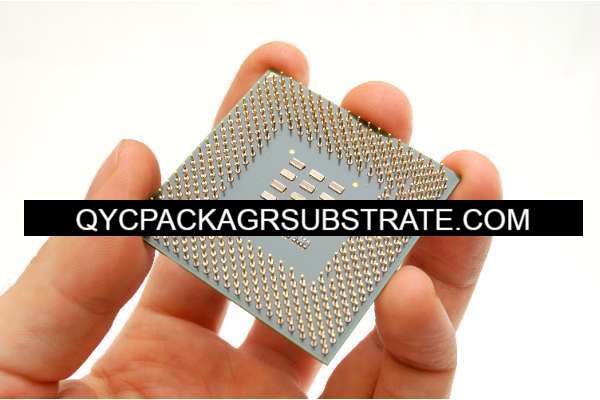
What Functions Does Semiconductor BGA Substrate Serve?
In the intricate world of electronic devices, the Semiconductor BGA (Ball Grid Array) substrate takes on the role of a versatile conductor, orchestrating a symphony of functions that define the performance and efficiency of the device. Let’s delve into the multifaceted roles played by these substrates:
Stage for IC Artistry: Picture the BGA substrate as a canvas for integrated circuits (ICs), providing a structured stage for their artistic prowess. Solder balls, arranged in a grid array, become the essential strokes securing the ICs in their dynamic performance.
Conductor of Connectivity Harmony: Beyond being a mere platform, the BGA substrate conducts a harmonious symphony of electrical connections. Solder balls, playing the dual role of mechanical anchors and electrical conduits, create a seamless connection between the integrated circuits and the broader electronic ensemble.
Signal Sonata: Weaving a melodious tapestry, the substrate establishes pathways for the smooth transmission of electrical signals. This ensures that the electronic conversation within the semiconductor device unfolds seamlessly, contributing to its overall melodic performance.
Thermal Balletic Movements: Amidst the electronic performance, BGA substrates gracefully execute a thermal ballet. Their composition and design allow for the elegant dissipation of heat generated by the ICs, preventing any overheating theatrics.
Architectural Choreographer: Beyond the electronic realm, these substrates take on the role of architectural choreographers. Much like supporting actors, they ensure the structural integrity of the semiconductor package, especially when the device encounters the dramatic twists of mechanical stress.
Efficiency Dance: Adding a touch of grace, BGA substrates contribute to the efficiency dance of electronic devices. The grid array configuration orchestrates a dance of solder balls, allowing for a high-density placement of connections within a confined space.
Integration Symphony: BGA substrates participate in a grand symphony of integration. They are not solo performers but rather integral components in the holistic packaging process, enabling the seamless integration of multiple ICs within a single electronic composition.
Automated Ballet Performance: Streamlining the production, BGA substrates gracefully perform in the automated ballet. Their uniform grid array, meticulously designed, seamlessly integrates with automated pick-and-place equipment during the manufacturing spectacle.
In essence, Semiconductor BGA substrates emerge as versatile conductors orchestrating a complex and harmonious performance, blending mechanical support, electrical connectivity, thermal management, and efficiency to create a symphony of advanced electronic devices.
What Are the Different Types of Semiconductor BGA Substrate?
Embarking on the journey into the realm of semiconductor BGA (Ball Grid Array) substrates unveils a tapestry of diverse types, each intricately designed to meet specific needs within the vast landscape of electronics. Let’s embark on an exploration of the various characters in this substrate saga:
Organic Overture:
FR-4: This ubiquitous organic substrate, woven from flame-retardant fibers, emerges as a cost-effective solution for a multitude of applications.
High-Temperature FR-4: Stepping into the spotlight with resilience, this variant withstands elevated temperatures, catering to applications with heightened thermal demands.
Ceramic Chronicles:
Alumina (Al2O3): The ceramic luminary boasting stellar thermal conductivity finds its stage in high-power applications, where the graceful dissipation of heat takes center stage.
Aluminum Nitride (AlN): Another ceramic virtuoso, celebrated for its thermal prowess, takes the lead in applications where managing heat becomes an art.
Metal Core Sonata:
Aluminum PCB: A metal core symphony, predominantly choreographed by aluminum, dances into the limelight, offering enhanced thermal performance. Its graceful moves are particularly sought after in applications like LED lighting.
Flex BGA Ballet:
Flexible Printed Circuits (FPC): The flexible virtuoso, capable of elegant bends and twists, graces the stage where non-planar surfaces beckon. Flex BGA substrates take the lead where flexibility and spatial constraints play a key role.
Composite Composition:
Polyimide-Based: The composite storyteller weaves tales of flexibility harmonizing with thermal resilience. These substrates, born of polyimide materials, find their place in applications that demand both flexibility and reliable thermal properties.
HDI Symphony:
Microvia Technology: In the high-density interconnect saga, microvia technology takes the lead, orchestrating a dance of increased circuit density and enhanced signal integrity. It shines in applications where the pursuit of miniaturization and high-density packaging is paramount.
PoP Extravaganza:
Multilayer PoP Substrates: A story of layers unfolds in the Package-on-Package drama, allowing for the vertical stacking of integrated circuits. This narrative finds resonance in mobile devices and scenarios where spatial constraints demand a vertical performance.
SiP Fusion:
Integrated SiP Substrates: In the System-in-Package ensemble, substrates play a pivotal role in integrating multiple functions within a singular package. A tale of efficiency and compact designs emerges in this SiP symphony.
In this grand narrative, the selection of a BGA substrate type is akin to casting characters for a play, where thermal requirements, electrical nuances, form factors, and budget considerations contribute to the creation of a harmonious electronic masterpiece. Semiconductor manufacturers, as the directors of this grand performance, carefully choose the substrate that best resonates with the unique demands of the electronic devices they envision.
How is Semiconductor BGA Substrate Connected to IC Packaging?
The intricate dance of semiconductor BGA (Ball Grid Array) substrates with integrated circuits (ICs) is a pivotal chapter in the story of IC packaging. Let’s delve into the nuanced connection and packaging process:
The Mounting Ballet:
BGA substrates provide a steadfast stage for the mounting of integrated circuits. The ICs gracefully take their positions, and the connection unfolds through solder balls or bumps, creating a robust and reliable mechanical bond.
Solder Ball Symphony:
The distinctive feature of BGA substrates is the array of solder balls beneath them. These balls act as both the architects of electrical connectivity and the maestros of mechanical attachment. Through the delicate dance of reflow soldering, a symphony of strong connections is orchestrated.
Flip-Chip Elegance:
In an alternative choreography, ICs may engage in a flip-chip bonding performance. The IC elegantly flips and rests face-down on the substrate, aligning solder bumps with corresponding pads. Reflow soldering ensues, creating direct electrical connections with a touch of artistic finesse.
Signal Waltz:
BGA substrates are adorned with intricate patterns of conductive traces, tracing a waltz of electrical signals. These traces intricately weave pathways for data, power, and other signals, ensuring a harmonious communication between the ICs and other components.
Power and Ground Pas de Deux:
The BGA substrate takes center stage in the distribution of power and ground connections to the ICs. Power and ground planes perform a pas de deux, ensuring a stable and efficient distribution of power throughout the electronic performance.
Thermal Pas de Trois:
A thermal ballet ensues, where the BGA substrate becomes a conduit for heat dissipation. Its material and design are curated to conduct and dissipate the heat generated by the ICs, ensuring a performance free from the overheating drama.
Symphony of Integration:
The BGA substrate is not a mere participant but a lead character in the grand symphony of IC packaging. It enables the integration of multiple ICs within a single package, ushering in a performance of compact and efficient design.
The connection between the BGA substrate and IC packaging is a choreographed masterpiece, involving intricate soldering techniques, signal routing choreography, and a dance of thermal considerations. This collaborative performance ensures that ICs seamlessly blend into the semiconductor package, delivering a captivating act of performance and reliability.
How Does Semiconductor BGA Substrate Differ from PCBs?
Within the electronic tapestry, Semiconductor BGA (Ball Grid Array) substrates and PCBs (Printed Circuit Boards) emerge as protagonists, each scripting a unique narrative in the grand story of technology. Let’s embark on an expedition to unearth the distinct nuances that characterize these two essential players:
Tailored Roles:
Semiconductor BGA Substrate: Assumes a specialized mantle, meticulously crafted to serve as the exclusive platform for the delicate choreography of mounting integrated circuits (ICs) within semiconductor packages. It is the designated stage where the dance of ICs and solder balls unfolds with intricate precision.
PCB: Casts a wider net, donning the mantle of the foundational architect for the entire electronic ensemble. It orchestrates a symphony of components, guiding their interconnected ballet across the expansive canvas of the entire system.
Choreography of Connectivity:
Semiconductor BGA Substrate: Graces the center stage with a choreography that intricately involves the direct mounting and connection of ICs. The dance of solder balls and bumps becomes a signature performance, marked by finesse and focus.
PCB: Extends an invitation to a diverse array of components, embracing a versatile choreography. Through soldering and interconnected pathways, it conducts a dynamic performance, allowing each component to showcase its unique moves in the electronic ballet.
Precision in Design:
Semiconductor BGA Substrate: Crafted with meticulous precision, its design showcases elaborate patterns of solder ball connections, signal traces, and power distribution—a visual masterpiece tailored exclusively for the art of IC mounting.
PCB: Paints a canvas with a broader stroke, considering the placement of a diverse cast of components. The design unfolds as a sophisticated tapestry, tracing signal routes that traverse the entire spectrum of the electronic narrative.
Adaptability and Size Spectrum:
Semiconductor BGA Substrate: Tailored with specificity, often residing in a smaller dimension, perfectly adapted to snugly fit within semiconductor packages—a bespoke stage set for the nuanced performance of ICs.
PCB: Demonstrates versatility in size, seamlessly adapting from compact to expansive dimensions. It becomes a stage adaptable to the varied needs of the electronic composition, accommodating an ensemble of components.
Unveiling Complexity:
Semiconductor BGA Substrate: While featuring multiple layers, it maintains an air of simplicity, channeling its complexity towards the precision required for the art of IC mounting—a focused and intricate performance.
PCB: Unveils a richer complexity, with multiple layers intricately choreographing signal routing, power distribution, and ground planes. The layers blend seamlessly to create a symphony of intricate connections across the entire system.
Symphony of Applications:
Semiconductor BGA Substrate: Takes a solo in the spotlight of semiconductor packaging applications, orchestrating the stage for the nuanced performance of ICs within their packages—an exclusive and specialized act.
PCB: Conducts a versatile symphony across a spectrum of applications, from the refined notes of consumer electronics to the robust crescendos of industrial systems—an orchestrator conducting the entire electronic composition.
In this grand tale of electronics, Semiconductor BGA substrates and PCBs step into the limelight with distinctive personas, contributing their unique narratives to the harmonious performance of the electronic symphony.
What are the Main Structure and Production Technologies of Semiconductor BGA Substrate?
In the enchanting world of Semiconductor BGA (Ball Grid Array) substrates, a rich tapestry of structures and cutting-edge production technologies unfolds, shaping the very essence of electronic ingenuity. Let’s embark on an exploration, delving into the diverse architectural nuances and the intricate choreography of production techniques that bring these substrates to life:
A Symphony of Architectures in Semiconductor BGA Substrates:
Organic Melody:
FR-4 Elegance: Behold the grace of BGA substrates woven from Flame Retardant-4 (FR-4) material, an exquisite epoxy-based laminate. This organic composition not only exudes elegance but also offers commendable electrical insulation, contributing to the symphony of reliability.
Ceramic Harmony:
Alumina’s Overture: Alumina ceramic substrates take the lead, unveiling an overture of excellent thermal conductivity. Perfect for applications that demand a seamless dance of efficient heat dissipation.
AlN Crescendo: Enter the crescendo with Aluminum Nitride (AlN) substrates, elevating the thermal conductivity to new heights. A stellar performance in applications with stringent thermal prerequisites.
Metal Core Ballet:
Aluminum PCBs Spotlight: The ballet of metal core substrates unfolds as BGA substrates with an aluminum core grace the stage. Witness an enhanced thermal performance that takes center stage, particularly applauded in applications like LED lighting.
Flexibility Waltz:
Flexible Printed Circuits Dance: The waltz of flexibility commences with BGA substrates adorned in the attire of Flexible Printed Circuits (FPC). With a graceful adaptability to non-planar surfaces, they become the prima donnas in applications like wearable devices.
Polyimide’s Tale:
Polyimide’s Balancing Act: Polyimide-based BGA substrates step into the limelight, narrating a tale of flexibility and thermal resilience. A harmonious balance tailored for applications seeking a blend of both attributes.
HDI’s Intricate Ballet:
Microvia’s Grandeur: High-Density Interconnect (HDI) BGA substrates take the spotlight, orchestrating a ballet of complexity through microvia technology. Witness an intricate dance of heightened circuit density and elevated signal integrity—a spectacle for enthusiasts of miniaturization.
The Artistry of Production Techniques:
Lamination Ballet:
Layers of copper foils and insulating materials engage in a ballet of lamination, crafting the foundational structure of BGA substrates with precision.
Etching Symphony:
The symphony of chemical etching takes center stage, sculpting the graceful patterns of traces that will carry electrical signals with artistic precision.
Drilling Precision:
Witness the precision drilling performance, creating pathways and microvias that seamlessly connect layers—a testament to the symphonic harmony of electrical pathways.
Solder Mask Elegance:
The stage is set for the elegance of solder mask application, leaving only the areas where soldering will unfold—a protective shield against short circuits, meticulously applied like strokes of a brush.
Surface Finish Mastery:
The surface takes on different finishes—a mastery of HASL, the opulence of ENIG, or the subtlety of OSP—each contributing to the artistry of soldering with a distinct flair.
Solder Ball Ballet:
Solder balls enter the limelight, precision-placed on the substrate. A ballet unfolds with solder paste and reflow soldering techniques—a choreography crafting the perfect connection performance.
Quality Control Symphony:
The grand symphony of quality control steps onto the stage—a visual inspection and testing spectacle ensuring that BGA substrates meet the stringent specifications for electrical prowess and reliability.
In the production theater of Semiconductor BGA substrates, the collaboration of diverse architectural notes and the precision dance of production techniques converge to create substrates that stand as works of art—each uniquely tailored for specific applications and destined to play a pivotal role in the electronic symphony.
Frequently Asked Questions (FAQs)
What Goes into the Production of Semiconductor BGA Substrates?
The production journey of Semiconductor BGA substrates involves intricate processes like lamination, etching, drilling, solder mask application, surface finish application (e.g., HASL, ENIG, OSP), solder ball placement utilizing solder paste and reflow soldering, and stringent quality control and testing.
How Do Solder Balls Contribute to BGA Substrate Functionality?
Solder balls on BGA substrates play a pivotal role, serving as vital connection points between the substrate and corresponding pads on the integrated circuit (IC). They seamlessly establish both electrical connectivity and mechanical attachment.
In Which Spheres Find Application for Semiconductor BGA Substrates?
Semiconductor BGA substrates find homes in diverse electronic devices, spanning consumer electronics, industrial equipment, automotive systems, medical devices, and more. Their compact and efficient packaging proves advantageous across an array of electronic applications.
What Advantages Do Ceramic BGA Substrates Offer?
Ceramic BGA substrates, crafted from materials like alumina or aluminum nitride, present advantages such as excellent thermal conductivity, fostering efficient heat dissipation. Their significance is accentuated in applications demanding heightened power requirements.
How Does HDI Technology Influence BGA Substrate Design?
The incorporation of High-Density Interconnect (HDI) technology in BGA substrates elevates circuit density and amplifies signal integrity. Microvia technology, seamlessly integrated, allows for intricate routing, contributing to both miniaturization and enhanced performance.
Are Flexible BGA Substrates Tailored for Wearable Devices?
Indeed, flexible BGA substrates, often rooted in flexible printed circuits (FPC) and polyimide materials, find a natural fit in wearable devices. Their flexibility enables seamless adaptation to the non-planar surfaces characteristic of wearable electronics.
Conclusion
In summary, the landscape of Semiconductor BGA (Ball Grid Array) substrates unfolds as a captivating narrative within the electronics realm. The curated set of Frequently Asked Questions (FAQs) has unraveled a tapestry of insights, spanning the gamut from substrate types and production intricacies to their versatile applications and inherent advantages.
These substrates, with their intricate diversity, boast compositions ranging from organic FR-4 materials to resilient ceramics like alumina and aluminum nitride, and innovative designs such as metal cores and flexible solutions. The production journey, akin to a well-orchestrated symphony, involves lamination artistry, precision etching, drilling finesse, and the delicate ballet of solder ball placement. Amidst this production symphony, the vigilant guardianship of quality control ensures each substrate meets the exacting standards of reliability and electrical performance.
Solder balls, the unsung heroes in this electronic narrative, emerge as crucial connectors, weaving the threads of electrical connectivity and mechanical attachment. The versatility of BGA substrates finds expression across a spectrum of electronic devices, from the ubiquitous consumer electronics to the robust machinery of industrial sectors, the intricate systems of automotive engineering, and the burgeoning landscape of wearable devices.
Ceramic BGA substrates, with their thermal prowess, carve a niche in applications demanding efficient heat dissipation. The integration of High-Density Interconnect (HDI) technology adds a crescendo to the design, enhancing circuit density and signal integrity—a key overture in the pursuit of miniaturization and elevated performance.
As the production curtain descends, these substrates take their well-deserved place at the forefront of the electronic symphony, contributing to technological advancements and innovations. The FAQs have not merely answered questions but have painted a vivid portrait of Semiconductor BGA substrates, casting them as foundational protagonists in the ever-evolving saga of electronic technology.