
Semiconductor FCBGA substrate Vender. High speed and high frequency material packaging substrate manufacturing. Advanced packaging substrate production process and technology.
The Semiconductor FC BGA Substrate is a specialized substrate used in semiconductor packaging, falling within the Ball Grid Array (BGA) category. BGA, as a packaging technology, establishes connections between the semiconductor device and the package through an array of solder balls strategically placed on the package’s underside.
In the domain of semiconductor packaging, the “FC” acronym is commonly attributed to “Flip Chip.” Flip Chip technology involves mounting the semiconductor die upside down, with connections made to the substrate or package using solder bumps or balls, a departure from traditional upright die mounting.
Thus, a Semiconductor FC BGA Substrate stands out for its integration of a BGA package configured with a Flip Chip arrangement. This substrate is preferred in advanced semiconductor devices for its advantages in electrical performance, efficient thermal management, and the overall reduction in the size of electronic components. Its importance lies in its pivotal role in the assembly and optimal functionality of integrated circuits and various semiconductor devices.
What is the function of Semiconductor FC BGA Substrate?
The Semiconductor FC BGA (Flip Chip Ball Grid Array) Substrate serves as a versatile cornerstone in semiconductor packaging, embracing a spectrum of functions that contribute to the efficacy and prowess of electronic devices:
Pivotal Connectivity Hub: Positioned as a central nexus, the substrate functions as a pivotal connectivity hub, forging electrical connections between the semiconductor device—often a flip chip—and the broader electronic system. This intricate linkage is facilitated by strategically placed solder balls on the substrate.
Meticulous Conductive Pathways: With intricate configurations of conductive traces, the substrate intricately constructs pathways for the smooth transmission of signals and power. These pathways facilitate seamless communication between the flip chip and other components on the printed circuit board (PCB).
Efficient Thermal Governance: A substantial responsibility of the substrate is the judicious regulation of heat generated during the semiconductor device’s operation. Through the provision of efficient thermal pathways, it orchestrates the dissipation of heat, precluding overheating and contributing to sustained device performance and reliability.
Stalwart Structural Support: Extending beyond its electrical duties, the substrate provides stalwart structural support to the flip chip. Functioning as a protective shield, it safeguards the chip from mechanical stresses and environmental elements, fortifying the overall mechanical resilience of the semiconductor package.
Sculpted for Space Efficiency: The adoption of a Flip Chip configuration on the BGA substrate inherently bequeaths a design that is both space-efficient and compact. This inherent trait proves advantageous in applications where considerations of size and weight take precedence.
Amplified Electrical Performance: The direct connection sans wire bonding between the flip chip and the substrate results in abbreviated electrical paths. This intentional design choice leads to amplified electrical performance, minimizing signal delays, and heightening the overall speed of the device.
In summation, the Semiconductor FC BGA Substrate emerges as a dynamic linchpin in semiconductor packaging, seamlessly harmonizing functions related to electrical connectivity, thermal governance, structural robustness, and design finesse.
What are the different types of Semiconductor FC BGA Substrate?
Semiconductor FC BGA (Flip Chip Ball Grid Array) Substrates exhibit diverse types, each meticulously crafted for distinct design, material, and application needs. Explore these categories:
Single-Layer Substrate: Simple yet effective, this type features a lone material layer with conductive traces on one side. It is a fitting choice for straightforward applications and is often employed in less intricate electronic devices.
Multilayer Substrate: Elevating complexity, multilayer substrates involve the stacking of multiple material layers, each adorned with conductive traces. This design facilitates intricate signal and power routing, making it a staple in advanced electronic devices with complex circuitry.
High-Density Interconnect (HDI) Substrate: Engineered for efficiency, HDI substrates leverage advanced manufacturing techniques to achieve finer pitch, smaller vias, and heightened circuit density. They are the go-to for applications where spatial efficiency takes precedence.
Ceramic Substrate: Embracing heat with grace, ceramic substrates utilize materials like alumina or aluminum nitride for excellent thermal conductivity. They shine in applications demanding effective heat dissipation, such as in power electronics.
Flexible Substrate: Bending the norms, flexible substrates are fashioned from materials that allow flexibility. They find their niche in applications where adaptability is key, like wearable electronics or devices with curved surfaces.
Organic Substrate: Grounded in cost-effectiveness, organic substrates, often crafted from fiberglass-reinforced epoxy, are versatile and widely deployed across various electronic devices.
Embedded Substrate: Merging seamlessly, embedded substrates integrate passive components directly into the substrate, yielding a more compact and space-efficient solution.
Specialized Substrates: Tailored precision, specialized substrates cater to specific needs, be it high-frequency applications, automotive electronics, or challenging environmental conditions.
In essence, the choice of substrate type is a meticulous dance with the unique demands of the electronic device, considering factors like performance nuances, spatial constraints, and thermal intricacies. The semiconductor industry perpetually unveils innovative substrate technologies, aligning seamlessly with the dynamic requirements of advancing electronic applications.
What is the relationship between Semiconductor FC BGA Substrate and IC packaging?
The intricate interplay between Semiconductor FC BGA (Flip Chip Ball Grid Array) Substrate and IC (Integrated Circuit) packaging forms a symbiotic synergy within the realm of semiconductor technology.. This alliance unfolds through various pivotal dimensions:
Mounting Dynamics: Semiconductor FC BGA Substrate introduces the innovative concept of flip chip mounting, where the semiconductor die is inverted and directly affixed to the substrate or package. This unconventional flip chip arrangement serves as the keystone in the design tapestry of IC packaging.
Electrical Nexus: At its core, the substrate acts as a conduit, weaving electrical connections between the flip chip and the broader electronic ecosystem. This foundational role assumes paramount importance in IC packaging, orchestrating the seamless transmission of signals and power between the integrated circuit and external circuitry.
Thermal Symphony: Both Semiconductor FC BGA Substrate and IC packaging coalesce in their shared commitment to thermal management. The substrate, particularly in a flip chip configuration, assumes a central role in the choreography of heat dissipation from the semiconductor device. Prudent thermal regulation becomes imperative for sustaining the performance and longevity of the integrated circuit.
Spatial Optimization: Embracing the ethos of miniaturization, the integration of flip chip technology on a BGA substrate seamlessly aligns with the industry’s pursuit of compact and space-efficient IC packaging. This collaboration becomes pivotal in the modern electronics landscape, where devices incessantly strive for smaller form factors and heightened portability.
Guardianship and Structural Harmony: The substrate, stepping into a role akin to a guardian, provides protective shielding and structural fortitude to the flip chip within Semiconductor FC BGA Substrate. This custodial function emerges as equally critical in IC packaging, acting as a shield against mechanical stresses and environmental influences, thereby upholding the structural integrity of the packaged device.
Pioneering Packaging Technologies: Semiconductor FC BGA Substrate stands as a symbol of advanced packaging technologies within the expansive canvas of IC design. The deliberate selection of substrate types, whether single-layer, multilayer, or specialized, reflects strategic considerations in the broader landscape of advanced IC packaging.
In essence, the interplay between Semiconductor FC BGA Substrate and IC packaging unfolds as a nuanced collaboration, where each element contributes harmoniously to the amalgamation of electronic components. This collaboration accentuates aspects of electrical connectivity, thermal equilibrium, structural resilience, and the holistic performance of integrated circuits, navigating the dynamic landscape of contemporary electronic devices.
What are the differences between Semiconductor FC BGA Substrate and PCB?
Within the intricate symphony of electronic systems, Semiconductor FC BGA (Flip Chip Ball Grid Array) Substrate and PCB (Printed Circuit Board) emerge as distinct instrumentalists, each meticulously attuned to play unique melodies. Let’s explore the nuanced harmonies that set them apart:
Function and Purpose:
Semiconductor FC BGA Substrate: This specialized virtuoso takes center stage in the orchestration of mounting and interconnecting semiconductor devices. Particularly skilled in configurations like flip chip mounting, it leads the ensemble in establishing electrical connections, managing thermal intricacies, and providing essential structural support to semiconductor components.
PCB: Part of a broader orchestral arrangement, the PCB assumes the role of a versatile conductor that supports and interconnects an ensemble of electronic components. Serving as the maestro in electronic devices, it forms the foundational architecture for arranging and interlinking various elements, including semiconductors, resistors, and capacitors.
Scope of Application:
Semiconductor FC BGA Substrate: Takes a solo spotlight in semiconductor packaging, especially in advanced setups leveraging flip chip technology. This specialized virtuoso is finely tuned for seamlessly integrating semiconductor devices.
PCB: Performs across the spectrum of electronic devices and applications, playing a crucial role in the symphony. From everyday consumer electronics to intricate industrial machinery, PCBs compose the backbone.
Component Integration:
Semiconductor FC BGA Substrate: Specializes in the nuanced integration of semiconductor devices, offering a purpose-driven platform for mounting and establishing connections with these components.
PCB: Embodies a comprehensive array of electronic components, including semiconductors, resistors, capacitors, connectors, and more. It serves as a versatile canvas for orchestrating and interconnecting diverse elements within an electronic system.
Complexity and Layering:
Semiconductor FC BGA Substrate: Adapts to varying complexities, capable of performing as a soloist or as part of an ensemble with multiple layers. Its design intricacies are finely tuned to meet the specific demands of semiconductor packages.
PCB: Conducts a variable complexity composition, featuring arrangements that span from solo performances to intricate multilayer symphonies. PCBs are composed to harmonize with the diverse intricacies of electronic system design.
Usage in Packaging:
Semiconductor FC BGA Substrate: Takes the lead in the realm of advanced semiconductor packaging, particularly in scenarios where the graceful efficiency of flip chip technology is harnessed for a refined and compact device design.
PCB: Assumes the pivotal role of the conductor, orchestrating the packaging and interconnection of an eclectic mix of electronic components within a system. It provides both structural robustness and electrical connectivity for the entire electronic performance.
In essence, while both Semiconductor FC BGA Substrate and PCB are indispensable instrumentalists in the electronic symphony, the former specializes in a solo act of semiconductor packaging with a meticulous focus on specific devices, whereas the latter conducts a versatile symphony as a foundational instrumentalist applied across a broad spectrum of electronic applications.
What is the main structure and production technology of Semiconductor FC BGA Substrate?
The Semiconductor FC BGA (Flip Chip Ball Grid Array) Substrate exhibits a complex structure, intricately woven with diverse elements, while its production technology is a fusion of precision and advanced manufacturing processes. Let’s explore the distinctive composition and manufacturing techniques in a unique narrative:
Unique Composition of Semiconductor FC BGA Substrate:
Foundation in Material Mastery:
Forging its identity from high-performance materials, be it the stalwart FR-4 (Fiberglass-Reinforced Epoxy) or the avant-garde BT (Bismaleimide Triazine) resin, the substrate material lays the groundwork for the intricate dance of electrons.
Dielectric Ballet:
The substrate comes alive with multiple dielectric layers, akin to layers in a ballet performance. These layers, gracefully positioned, harmonize to provide insulation, contributing to the electrical performance and signal clarity of the substrate.
Traces of Conductive Elegance:
Etched onto the substrate with a touch of artistic flair, the conductive traces form a mesmerizing pattern. These traces act as the virtuosos, conducting electrical signals in a choreographed dance between the flip chip and other components.
Via Structures:
The substrate’s architecture features metal-plated vias, reminiscent of architectural pillars. These vias create a vertical symphony, allowing the substrate to transcend into a multilayered masterpiece, seamlessly connecting different layers.
Solder Mask Veil:
A protective veil, akin to a masked ball, the solder mask is delicately applied. This layer shields the conductive traces, leaving openings strategically placed for soldering. It adds a touch of mystique to the substrate during the soldering process.
BGA Grand Finale:
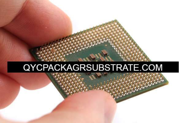
Beneath the surface, the BGA component takes center stage, flaunting an array of solder balls. These solder balls, like a grand finale, serve as connection points, forging a harmonious connection between the substrate and the PCB or other electronic components.
Narrative of Production Technology:
Design Symphony:
The production unfolds with a symphony of design, a composition orchestrated by engineers. The arrangement of traces, via structures, and features is akin to crafting a musical score tailored to the nuances of the semiconductor device.
Material Sonata:
Material selection becomes a sonata, where engineers harmonize thermal dynamics, signal integrity, and budget considerations. The chosen materials become instrumental in creating a seamless blend of form and function.
Artistry in Manufacturing Ballet:
The manufacturing process emerges as a ballet of artistry, where layers are delicately layered, laminated, and the application of conductive traces is executed with the precision of a choreographed dance.
Solder Mask Waltz:
The solder mask takes on the elegance of a waltz, whether applied through screen printing or photolithography. It becomes a dance of protection and aesthetics, contributing to the overall allure of the substrate.
BGA Ball Attachment Opera:
The attachment of solder balls in the BGA component transforms into a captivating opera. Precision becomes the key performer, ensuring not just functional connections but a visually stunning alignment that captivates the audience.
Quality Crescendo:
The production reaches its zenith with a crescendo of quality control measures, reminiscent of a musical climax. Rigorous testing becomes the critical performance review, ensuring that every note, or in this case, every component, contributes to the overall harmony.
In essence, the Semiconductor FC BGA Substrate is not just a technological marvel but a symphony of elements, where composition and manufacturing techniques converge to create an intricate dance of functionality and reliability.
FAQs (Frequently Asked Questions)
What is the role of conductive traces in Semiconductor FC BGA Substrate?
Conductive traces within the substrate form intricate pathways, facilitating the smooth transmission of signals and power between the flip chip and other components on the printed circuit board (PCB). They are integral to establishing reliable electrical connections.
How is the manufacturing process of Semiconductor FC BGA Substrates conducted?
The manufacturing process involves phases such as design and layout, careful selection of substrate materials, application of printed circuit board manufacturing techniques, precision application of solder mask, attachment of BGA balls, and rigorous quality control and testing.
What role does the Ball Grid Array (BGA) play in Semiconductor FC BGA Substrate?
The BGA component, featuring an array of solder balls on the substrate’s underside, serves as critical connection points. These solder balls facilitate the attachment of the substrate to the PCB or other electronic components, ensuring a reliable and space-efficient connection.
In which semiconductor devices is Semiconductor FC BGA Substrate most beneficial?
Semiconductor FC BGA Substrates are particularly advantageous in advanced semiconductor packaging scenarios, especially those leveraging flip chip technology. They find application in devices where compact design, effective thermal management, and efficient electrical connections are paramount.
How does the production technology ensure the reliability of Semiconductor FC BGA Substrates?
The production technology employs precise engineering, meticulous material selection, and rigorous quality control measures. Thorough testing is conducted to ensure the reliability of electrical continuity, solder joint quality, and overall performance of the Semiconductor FC BGA Substrate.
Conclusion
In a nutshell, the Semiconductor FC BGA (Flip Chip Ball Grid Array) Substrate emerges as a key player in the intricate dance of semiconductor technology. With its intricate structure crafted from high-performance materials, adorned with precise conductive traces and via structures, it takes on the vital role of orchestrating seamless electrical connections and providing a robust platform for mounting semiconductor devices.
Diverging from the beaten path of traditional PCBs, the Semiconductor FC BGA Substrate showcases its prowess in advanced semiconductor packaging, especially in configurations embracing flip chip technology. The BGA component, bedecked with an array of solder balls, steps into the spotlight, facilitating reliable and space-efficient connections to the PCB and other electronic components.
The manufacturing process unfolds like a carefully choreographed performance, where precision in design, thoughtful material selection, and an unwavering commitment to quality control measures perform a harmonious symphony. From the inception of substrate materials to the delicate dance of solder mask application, each manufacturing step contributes to the overall reliability and performance of the Semiconductor FC BGA Substrate.
In the expansive landscape of semiconductor devices, this specialized substrate finds its groove in applications where compact design, efficient thermal management, and precise electrical connections take the lead. As technology propels forward with unbridled enthusiasm, the Semiconductor FC BGA Substrate remains an indispensable cornerstone, shaping the course of electronic systems and playing a pivotal role in bringing cutting-edge semiconductor devices to life.