
Semiconductor Packaging Substrate Vender. the Package Substrate will be made with Showa Denko and Ajinomoto High speed materials.or other types high speed materials and high frequency materials.
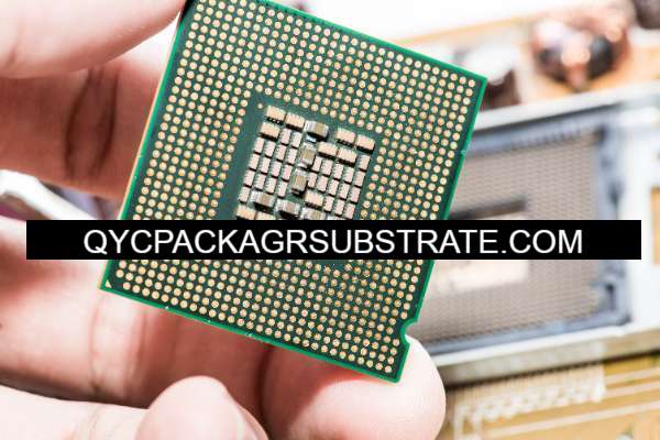
A Semiconductor Packaging Substrate is a crucial component used for carrying and connecting chips (integrated circuits).It plays a vital role in semiconductor packaging by facilitating electrical connections, offering mechanical support, and aiding in thermal dissipation.
Semiconductor packaging substrates are commonly crafted from insulating materials, including organics like epoxy resin or inorganics such as ceramics. These materials form the basis for establishing electrical connections, offering mechanical support, and aiding in thermal dissipation within semiconductor devices. Their key roles encompass:
Electrical Connections: Semiconductor chips need to establish connections with diverse electronic elements, such as resistors and capacitors, in addition to interfacing with external circuits.The packaging substrate acts as a foundation for these electrical connections, enabling the chip to link with external circuits using methods such as wires, solder balls, or other connection technologies.
Mechanical Support: The packaging substrate offers physical support to the chip, helping protect it from mechanical stress and vibrations. This is crucial for ensuring the reliability and stability of the chip.
Thermal Dissipation: During operation, chips generate heat. Packaging substrate designs typically incorporate heat dissipation structures to efficiently transfer heat to the surrounding environment, preventing chip overheating and performance degradation.
The type and design of semiconductor packaging substrates vary based on applications and performance requirements. Some common types of packaging substrates include Ball Grid Array (BGA), Chip-on-Board (COB), Multi-Chip Module (MCM), and others. These substrates play a critical role in electronic devices, enabling chips to function effectively in practical applications.
What Functions Does Semiconductor Packaging Substrate Serve?
Semiconductor packaging substrate plays a crucial role in semiconductor devices, serving various functions. Here are some of the primary functions:
Electrical Connection: The packaging substrate provides electrical connections between the semiconductor chip and external circuits. Through wires, solder balls, or other connecting elements on the substrate, the chip can be linked to other components on the circuit board.
Mechanical Support: The packaging substrate offers physical support and protection to the chip. This prevents potential harm to the chip caused by mechanical stress or vibrations, ensuring the stability of the device.
Heat Dissipation: In some cases, the packaging substrate is used for heat dissipation, aiding in transferring the heat generated by the chip to the surrounding environment to prevent overheating and its impact on device performance.
Signal Transmission: The substrate facilitates signal transmission through its internal wires and interlayer connections. This is crucial for transferring data and signals between different functional blocks within the chip.
Packaging Protection: The substrate can provide environmental protection for the chip, guarding against dust, moisture, and other environmental factors.
Size and Shape Adaptation: The design of the packaging substrate can meet various size and shape requirements to accommodate different application scenarios and device forms.
Multilayer Design: Some packaging substrates are designed with multiple layers, allowing for the vertical integration of multiple functions and increasing the device’s level of integration.
In summary, the packaging substrate in semiconductor devices plays multiple roles, including connection, support, heat dissipation, and protection, all of which are crucial for the device’s performance and stability.
What Types of Semiconductor Packaging Substrate Exist?
What types of semiconductor packaging substrates exist? Here are some common types:
Ball Grid Array (BGA): BGA is a packaging technique involving a grid array of solder balls positioned underneath the package, aiming to boost connection density and enhance heat dissipation.
Chip-on-Board (COB): COB technology directly affixes a chip onto a circuit board, eliminating the necessity for a traditional packaging shell and establishing a direct link between the chip and the circuit board.
Multi-Chip Module (MCM): MCM, as a packaging format, enables the integration of multiple chips within a single package, thereby improving both integration and overall performance.
Dual In-Line Package (DIP): DIP is a traditional packaging form where the chip’s pins are distributed on two sides in two rows, inserted into holes on the circuit board for connection.
Leadless Package: Leadless packaging is an environmentally friendly packaging technology that reduces environmental impact by using lead-free solder or other eco-friendly materials.
Plastic Packaging: This involves using plastic as the packaging material, commonly found in applications with lower costs.
These are just some types of semiconductor packaging substrates, and there are many other forms based on specific application requirements, performance standards, and manufacturing technologies.
How Does Semiconductor Packaging Substrate Differ from Traditional PCBs?
Semiconductor packaging substrates differ from traditional printed circuit boards (PCBs) in several significant aspects:
Technical Requirements: Semiconductor packaging substrates typically need to meet higher technical requirements as they directly interface with sensitive semiconductor chips. This includes higher density, smaller dimensions, finer line widths/spacings, and more advanced manufacturing processes.
Layered Structure: Semiconductor packaging substrates are often designed with multiple layers and a more complex hierarchical structure to accommodate multiple electrical connections, power planes, and ground planes. In contrast, traditional PCBs may be relatively simpler.
Material Selection: Semiconductor packaging substrates commonly employ high-performance materials such as high-temperature ceramics or organic packaging materials to meet the elevated environmental requirements of semiconductor devices, including temperature and humidity. Traditional PCBs may use more conventional materials like FR-4 (fiberglass-reinforced epoxy resin).
Manufacturing Processes: The manufacturing process for semiconductor packaging substrates is relatively intricate, often involving precision techniques such as gold plating and tin plating to ensure reliable electrical connections. Conversely, the manufacturing process for conventional PCBs is typically less complex.
Application Areas: Semiconductor packaging substrates are mainly employed for the encapsulation and interconnection of semiconductor chips. In contrast, traditional PCBs find broader application in supporting and linking a variety of electronic components, including resistors, capacitors, and integrated circuits.
Cost: The elevated specifications and intricate manufacturing processes associated with semiconductor packaging substrates typically result in higher production costs when compared to traditional PCBs.
To summarize, semiconductor packaging substrates are crafted with precision to cater to the specialized requirements of semiconductor devices, while traditional PCBs find application across a wider spectrum in general electronic circuits.
What Comprises the Structure and Production Technologies of Semiconductor Packaging Substrate?
The structure and production technologies of semiconductor packaging substrate comprise the following elements:
Substrate Material: The typical composition of the substrate involves insulating materials, which may include organic substrates like epoxy resin or inorganic substrates such as ceramics. The choice of substrate material depends on application requirements, heat dissipation performance, and manufacturing costs.
Electrical Connections: The design of the packaging substrate involves the layout of electrical connections, including wires, solder balls, etc., connecting the chip to external circuits. Common electrical connection technologies include micro-pin connections, Ball Grid Array (BGA), and others.
Heat Dissipation Structures: To facilitate effective heat dissipation, packaging substrates often incorporate heat dissipation structures such as heat pads, heat layers, or heat holes. This helps transfer the heat generated during chip operation to the surrounding environment.
Layered Structure: Packaging substrates may consist of multiple layers, each serving specific functions such as signal layers, power layers, and ground layers. Multilayer structures contribute to increased circuit complexity and integration.
Printed Circuit Board (PCB) Manufacturing Technology: The production of packaging substrates typically involves PCB manufacturing technologies, including processes such as photolithography, etching, deposition, and copper plating. These steps are used to form electrical connections and layered structures.
Packaging Process: Manufacturing semiconductor packaging substrates also involves the packaging process, which includes placing the chip on the substrate, connecting, encapsulating, testing, and other steps.
These elements collectively form the structure and production technologies of semiconductor packaging substrates, ensuring their crucial role in electronic devices.
How Are Chip Package Technologies Classified?
Chip package technologies can be classified based on various features and applications. Here are some common classification criteria:
Packaging Types:
Bare Die Packaging: Directly encapsulating the chip, often used in high-density and high-performance applications.
Chip-on-Board Packaging: Connecting the chip directly to the circuit board, providing a compact solution.
Transistor Outline Packaging: Encapsulation using metal casings, such as TO-220, TO-92, etc.
Plastic Packaging: Using plastic materials for encapsulation, such as QFP (Quad Flat Package), SOIC (Small Outline Integrated Circuit), etc.
Pin Layout:
Single In-Line Package (SIP): Pins are arranged in a single row.
Dual In-Line Package (DIP): Pins are arranged in two parallel rows.
Surface Mount Device (SMD): Pins are surface-mounted onto the circuit board, e.g., QFN (Quad Flat No-leads), BGA (Ball Grid Array), etc.
Packaging Materials:
Ceramic Packaging: Using ceramic materials, offering excellent heat dissipation, suitable for high-temperature environments.
Plastic Packaging: Using plastic materials, relatively lower in cost, suitable for general applications.
Package Size:
Micro-Packaging: Designed for miniaturization and lightweight applications, e.g., Chip Scale Package (CSP).
Large-Packaging: Designed for high power and high-performance applications, e.g., Pin Grid Array (PGA).
Heat Dissipation Techniques:
Active Cooling Packaging: Integrates cooling devices like fans or heat sinks.
Passive Cooling Packaging: Relies on external heat dissipation methods, such as heat spreaders or thermal compounds.
Application Areas:
Automotive Packaging: Meets specific requirements for the automotive industry, such as high-temperature resistance and vibration resistance.
Wireless Communication Packaging: Tailored to the specific needs of mobile devices and communication equipment.
These classification criteria may sometimes overlap and depend on specific technologies and market demands.
Frequently Asked Questions (FAQs) About Semiconductor Packaging Substrate
What is a semiconductor packaging substrate?
A semiconductor packaging substrate serves as a crucial material in encapsulating and linking semiconductor chips. It plays a vital role by facilitating electrical connections, offering mechanical support, dissipating heat, and providing protection. These functions are essential for ensuring the optimal performance of semiconductor devices.
What are the main functions of semiconductor packaging substrates?
The main functions include providing electrical connections, supporting semiconductor chips, dissipating heat, transmitting signals, and offering packaging protection. These functions contribute to ensuring the stability and reliability of the device.
How does a semiconductor packaging substrate differ from traditional PCBs?
Semiconductor packaging substrates focus on meeting the specific requirements of semiconductor devices, including higher technical demands, complex hierarchical structures, and elevated environmental requirements. Traditional PCBs are generally used in general electronic applications with simpler designs.
What are common materials used for packaging substrates?
Common packaging substrate materials include ceramics, organic packaging materials, and high-performance plastics. Material selection depends on application requirements such as temperature range, heat dissipation performance, etc.
What is the manufacturing process of semiconductor packaging substrates?
The manufacturing process involves several steps, including substrate material selection, circuit design, printed circuit board manufacturing, chip packaging, soldering, and testing. Each step influences the final product’s performance.
What are the key factors in the design of packaging substrates?
Key factors include the design of electrical connections, hierarchical structure, heat dissipation design, size and shape adaptation, material selection, and special design considerations for meeting specific application requirements.
What are the future trends in the development of semiconductor packaging substrates?
Future trends may include higher integration packaging, advanced heat dissipation technologies, environmentally friendly material choices, and customized designs for emerging applications such as 5G and the Internet of Things (IoT).
In which areas of the electronics industry are packaging substrates widely applied?
Packaging substrates are widely used in telecommunications, computing, consumer electronics, automotive electronics, medical devices, and various other fields, providing crucial support and connectivity functions for a variety of electronic devices.
In Conclusion
In conclusion, semiconductor packaging substrates play a crucial role in electronic devices. The structure and production technologies involve the selection of substrate materials, the design of electrical connections, consideration of heat dissipation structures, configuration of multilayer structures, and the use of printed circuit board manufacturing technology and packaging processes, among other steps. Different types of packaging substrates are suitable for various applications and are chosen based on specific requirements and performance standards. Through continuous technological innovation and manufacturing optimization, semiconductor packaging substrates not only enhance the performance and reliability of electronic devices but also contribute to the overall development of the semiconductor industry.