
Semiconductor package and Semiconductor Substrate Manufacturer. We use advanced Msap and Sap technology, High multilayer interconnection substrates from 2 to 20 layers.
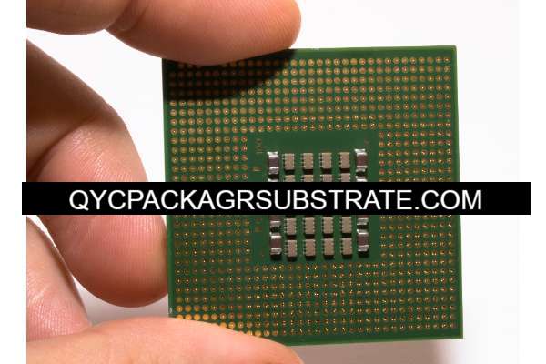
A semiconductor package substrate is a crucial component in semiconductor packaging technology, used to support and connect chips to external circuits. It is a material that provides mechanical support, electrical connections, and thermal performance. Semiconductor package substrates are typically made of conductive materials, usually metals, to facilitate the transmission of signals and power between the chip and external devices.
The primary functions of the package substrate include:
Mechanical Support: Providing physical support to the chip to prevent it from being affected by mechanical stress and vibration.
Electrical Connections: Offering electrical connections to enable communication between the chip and external circuits. This often involves transmitting signals through metal lines or other conductive structures on the package substrate.
Thermal Dissipation: Assisting in chip cooling to prevent overheating damage. Some package substrate designs incorporate heat-dissipating structures, such as heat sinks or thermal vias, to enhance thermal performance.
Packaging and Protection: The package substrate plays a role in shielding the chip from external environmental factors like humidity, dust, and contaminants, providing an additional layer of protection for the semiconductor.
The selection of a package substrate is contingent upon the distinct needs of the application, encompassing packaging technology, thermal specifications, electrical performance, and additional considerations. Within the semiconductor industry, diverse package substrates exist, including but not limited to Ball Grid Array (BGA), Chip Scale Package (CSP), Dual In-Line Package (DIP), among others.The design and material selection of these substrates are influenced by manufacturers and application needs.
What Functions Does Semiconductor Package Substrate Fulfill?
A semiconductor package substrate serves various functions and is a crucial component in semiconductor packaging technology. These functions include:
Mechanical Support: Providing physical support to prevent the chip from being affected by mechanical stress and vibrations.
Electrical Connections: Offering electrical connections to facilitate the transmission of signals and power between the chip and external circuits.
Thermal Dissipation: Assisting in the chip’s thermal dissipation to prevent overheating damage. Some package substrate designs incorporate heat-dissipating structures, such as heat sinks or thermal vias, to enhance thermal performance.
Packaging and Protection: Contributing to the encapsulation of the chip, shielding it from the impact of humidity, dust, and other contaminants, thereby enhancing the durability and reliability of the chip.
These functions make the semiconductor package substrate an indispensable component for the normal operation of semiconductor devices. The design and selection of package substrates depend on specific application requirements and packaging technologies. Different types of package substrates, such as Ball Grid Array (BGA), Chip Scale Package (CSP), and Dual In-Line Package (DIP), offer diverse choices to meet various application needs.
What Are the Different Types of Semiconductor Package Substrate?
There are various types of semiconductor package substrates, mainly determined by their design and intended use. Here are some common types of semiconductor package substrates:
Ball Grid Array (BGA): BGA substrates utilize spherical solder balls to connect the chip to the substrate, providing high electrical and thermal performance. Due to their dense array of solder balls, BGAs are widely used in high-performance integrated circuit packaging.
Chip Scale Package (CSP): CSP substrates are compact packages, often with the chip directly connected to the substrate, reducing the package’s size and weight. CSP is suitable for applications requiring thin and small form factors, such as mobile devices.
Dual In-Line Package (DIP): DIP substrates represent a traditional packaging form, where the chip’s pins are arranged in two rows for insertion and connection to a circuit board. While less common in high-density integrated circuits, DIPs are still used in some traditional applications.
Quad Flat No-Lead (QFN): QFN substrates are a type of leadless package with solder pads on the package’s bottom, aiding in improved thermal performance. QFNs are common in applications requiring enhanced heat dissipation.
3D Packaging: 3D packaging involves stacking multiple chips vertically, contributing to increased integration and performance of the package.
System-in-Package (SiP): SiP integrates multiple functional modules into a single package, potentially including processors, memory, wireless communication, and more.
These are just some examples of semiconductor package substrates, and there are many other types, each with its unique advantages and suitable scenarios. Choosing the appropriate substrate type typically depends on the specific requirements of the application, performance criteria, as well as design and manufacturing considerations.
How Does Semiconductor Package Substrate Differ from PCB?
Semiconductor Package Substrate and Printed Circuit Board (PCB) are distinct entities, each serving vital functions in electronic devices. Below are key distinctions between them:
Function and Purpose:
Semiconductor Package Substrate: Primarily used to support and connect chips, providing mechanical support, electrical connections, and thermal performance. It is a critical component for encapsulating chips, enabling communication with external circuits.
Printed Circuit Board (PCB): Mainly used to connect and support electronic components such as resistors, capacitors, integrated circuits, etc. It provides electrical connections between these components and mechanical support.
Composition and Materials:
Semiconductor Package Substrate: Typically composed of conductive materials, often metals, to support electrical connections and may include heat-dissipating structures.
Printed Circuit Board (PCB): Typically made of insulating materials, such as glass fiber-reinforced epoxy resin (FR-4), with copper layers forming conductive paths on the surface.
Connector Devices:
Semiconductor Package Substrate: Connects chips and packages, usually through soldering techniques like ball grid array (BGA) or chip scale package (CSP).
Printed Circuit Board (PCB): Establishes connections among diverse electronic components like resistors, capacitors, integrated circuits, etc., usually through soldering or plug-in interfaces.
Application Areas:
Semiconductor Package Substrate: Mainly applied in integrated circuit (IC) packaging, such as BGA, CSP, and other applications that involve encapsulating chips.
Printed Circuit Board (PCB): These elements find widespread use in diverse applications, including motherboards, power boards, and communication devices, providing connectivity and support for a variety of electronic components.
In essence, Semiconductor Package Substrate and Printed Circuit Board play distinct roles within electronic systems. While Semiconductor Package Substrate is primarily dedicated to encapsulating chips, the Printed Circuit Board serves the broader functions of offering comprehensive electrical connectivity and support for the entire electronic system.
What Comprises the Main Structure and Production Technologies of Semiconductor Package Substrate?
The main structure of a semiconductor package substrate consists of multiple layers, and its production technology involves several steps. Here is a general overview of the main structure and production technologies of semiconductor package substrates:
Main Structure:
Base Material Layer: The bottom layer of the semiconductor package substrate is typically the base material layer, providing mechanical support and the foundation structure. Common base materials include glass fiber-reinforced epoxy resin (FR-4) or other high-performance materials.
Conductive Layer: Above the base material layer, there is usually one or more layers of conductive material to achieve electrical connections. These conductive layers typically use copper and form circuit patterns through processes like chemical etching.
Dielectric Layer: Above the conductive layer, there is a dielectric layer that isolates different conductive layers to prevent short circuits. The material of the dielectric layer is usually insulating.
Solder Pads and Pins: On the top layer of the package substrate, there are solder pads and pins used to connect the chip to external circuits. Solder pads are a crucial part of connecting the chip through soldering techniques.
Heat Dissipation Structure: Some package substrate designs may include heat dissipation structures such as heat sinks or thermal vias to enhance thermal performance.
Production Technologies:
Printed Circuit Board Manufacturing Technology: Multilayer semiconductor package substrates often use printed circuit board (PCB) manufacturing technology. This involves stacking layers such as conductive layers, dielectric layers, and using processes like photolithography and etching to form circuit patterns.
Soldering Technology: The manufacturing of package substrates involves soldering techniques to connect chips and other components. This may include Surface Mount Technology (SMT) or Through-Hole Assembly (THA), depending on the type of packaging.
Thin Film Technology: Some advanced package substrates may employ thin film technology by applying thin films to achieve flexible or more complex circuit designs.
Heat Dissipation Technology: For packages requiring excellent heat dissipation, heat dissipation technologies may be employed, such as adding heat sinks, thermal adhesives, or other heat dissipation structures.
These are key aspects of the general structure and production technologies of semiconductor package substrates. The specific manufacturing processes and material choices vary based on application requirements and technical specifications.
Conclusion
Semiconductor package substrates play a crucial role in the electronics industry, and their significance is evident in several key aspects:
Support and Connection of Chips: Semiconductor package substrates serve as a robust support platform for chips, facilitating close connections between chips and external circuits through their electrical interconnections.
Mechanical Support: Beyond providing mechanical support on circuit boards, package substrates offer necessary protection to chips, helping prevent physical damage.
Thermal Performance: For high-performance chips, some package substrate designs consider heat dissipation structures to ensure efficient heat dissipation during operation, maintaining a stable working temperature.
Diverse Package Types: Various package substrate types, such as BGA, CSP, DIP, QFN, and others, exist to cater to diverse choices based on different application fields and performance requirements.
In summary, semiconductor package substrates are indispensable components in electronic devices. Their design and performance directly impact the performance of chips and the stable operation of the entire electronic system. Therefore, a profound understanding of the importance of semiconductor package substrates is crucial to ensuring the reliability and performance of electronic products.