
Showa Denko Package Substrate Manufacturer
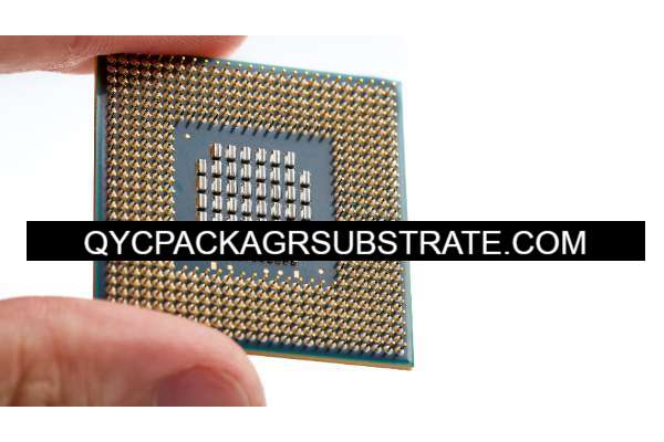
Showa Denko Package Substrate Manufacturer,Showa Denko Package Substrate is a high-performance packaging substrate designed to meet the stringent requirements of modern electronic devices. Utilizing advanced materials and processes, it offers excellent thermal conductivity and electrical performance, suitable for high-density and high-speed applications. Its stable structure is compatible with various chip packaging methods, such as BGA and CSP, making it widely used in semiconductor packaging and communication equipment. Showa Denko Package Substrate not only provides reliable signal transmission but also enhances overall device performance and durability, making it an ideal choice for high-performance electronic products.
What is a Showa Denko Package Substrate?
Showa Denko Package Substrate refers to a type of advanced material used in the production of semiconductor packages and integrated circuits (ICs). Showa Denko, a leading chemical company based in Japan, specializes in the development and manufacturing of various electronic materials, including package substrates.
These substrates play a crucial role in electronic packaging by providing a stable and reliable platform for mounting semiconductor chips. Showa Denko Package Substrates are known for their high thermal conductivity, excellent electrical insulation properties, and mechanical reliability. These characteristics are essential for ensuring the efficient operation and longevity of electronic devices, especially those in high-performance applications like servers, telecommunications equipment, and automotive electronics.
The design guidelines for Showa Denko Package Substrates typically emphasize factors such as thermal management, signal integrity, and manufacturability. They are engineered to handle the rigorous demands of modern electronic circuits, which often require compact designs with minimal signal loss and maximum heat dissipation capabilities.
Manufacturing processes for Showa Denko Package Substrates may include advanced techniques such as laser drilling, plating, and high-precision etching to achieve the desired electrical and mechanical properties. These substrates are often designed to meet specific customer requirements, offering customization options in terms of dimensions, layer configurations, and material compositions.
In summary, Showa Denko Package Substrates represent a cornerstone in the development of reliable and high-performance electronic devices, leveraging advanced materials and precise manufacturing processes to meet the evolving demands of the semiconductor industry.
Showa Denko Package Substrate Manufacturer
What are the Design Guidelines for Showa Denko Package Substrate?
The design guidelines for Showa Denko Package Substrates typically encompass several key aspects to ensure optimal performance and reliability in electronic applications. Here are some general design considerations:
- Material Selection:Choose the appropriate substrate material based on thermal conductivity, dielectric properties, and mechanical strength requirements. Showa Denko offers a range of materials with varying characteristics to suit different application needs.
- Layer Stackup Design: Define the layer stackup configuration considering signal integrity, power distribution, and thermal management requirements. Ensure adequate separation between signal and power planes to minimize noise and interference.
- Dimensional Accuracy: Specify precise dimensions and tolerances for the substrate to ensure compatibility with semiconductor chips and mounting processes. This includes considerations for package size, pad pitch, and alignment features.
- Thermal Management: Incorporate features such as thermal vias, metal-filled vias, and heat sinks to enhance thermal dissipation and prevent overheating of semiconductor devices. Ensure efficient heat transfer from the chip to the substrate and then to the external environment.
- Signal Integrity: Optimize trace routing and via placement to maintain signal integrity and minimize signal loss. Follow best practices for impedance control, signal routing symmetry, and minimizing electromagnetic interference (EMI).
- Manufacturability: Design with manufacturability in mind by considering capabilities such as laser drilling, precision etching, and plating processes. Ensure that the design can be reliably manufactured at scale with consistent quality.
- Reliability Considerations: Evaluate the substrate design for mechanical robustness, resistance to environmental factors (such as moisture and temperature variations), and long-term reliability under operational conditions.
- Testing and Validation:Plan for testing and validation of the substrate design to ensure it meets performance specifications and reliability targets. Consider simulations, prototypes, and reliability testing methodologies.
By adhering to these design guidelines, engineers can effectively leverage Showa Denko Package Substrates to achieve high-performance, reliable electronic assemblies suitable for a wide range of applications in industries such as telecommunications, automotive electronics, and consumer electronics.
What is the Fabrication Process for Showa Denko Package Substrate?
The fabrication process for Showa Denko Package Substrates typically involves several advanced steps to achieve the desired material properties and dimensional accuracy required for semiconductor packaging. Here’s an overview of the general fabrication process:
- Material Selection: The process begins with selecting the appropriate substrate material based on specific application requirements such as thermal conductivity, dielectric constant, and mechanical strength. Showa Denko offers a variety of materials tailored to different needs.
- Preparation of Substrate Material: The chosen substrate material undergoes preparation steps, which may include cleaning and surface treatment to ensure proper adhesion of subsequent layers and to remove contaminants that could affect material properties.
- Layer Formation and Lamination: The substrate material is processed to form multiple layers with precise thickness and composition. This involves techniques such as coating, deposition (e.g., chemical vapor deposition), and lamination to build up the desired layer stackup.
- Circuit Patterning: Photolithography and etching processes are used to define circuit patterns on the substrate layers. This step involves applying a photoresist layer, exposing it to UV light through a mask with the desired circuit pattern, developing the resist to reveal the pattern, and then etching away the exposed areas to create the circuit traces.
- Via Formation: Vias (electrical connections between layers) are created using techniques like laser drilling or mechanical drilling followed by metallization (typically through processes like sputtering or electroplating) to establish electrical continuity between different layers.
- Surface Finish: The substrate’s surface may undergo treatment to apply a suitable finish for soldering processes, ensuring good solder joint reliability during semiconductor chip attachment.
- Quality Assurance and Testing: Throughout the fabrication process, quality control measures are implemented to monitor material properties, dimensional tolerances, and adherence to design specifications. Testing methodologies may include dimensional inspection, electrical testing, and reliability testing under simulated operating conditions.
- Final Inspection and Packaging:Once fabrication is complete and the substrates pass quality assurance checks, they are inspected for defects and prepared for packaging according to customer requirements.
The specific details of each step in the Showa Denko Package Substrate fabrication process may vary depending on the exact substrate material and design specifications. Advanced manufacturing techniques and stringent quality control ensure that these substrates meet the high standards required for reliable semiconductor packaging in various industries.
How is a Showa Denko Package Substrate Manufactured?
The manufacturing process of a Showa Denko Package Substrate involves several intricate steps to ensure high performance and reliability in semiconductor packaging. Here’s a detailed overview of the typical manufacturing process:
- Material Selection: Begin by selecting the appropriate substrate material based on specific requirements such as thermal conductivity, dielectric properties, and mechanical strength. Showa Denko offers a range of materials tailored to different applications.
- Preparation of Substrate Material: The selected substrate material undergoes preparation steps, including cleaning and surface treatment. This ensures proper adhesion of subsequent layers and removes contaminants that could affect material properties.
- Layer Formation and Lamination: Process the substrate material to form multiple layers with precise thickness and composition. This involves techniques like coating, deposition (e.g., chemical vapor deposition), and lamination to build the desired layer stackup.
- Circuit Patterning: Utilize photolithography and etching processes to define circuit patterns on the substrate layers. This includes applying a photoresist layer, exposing it to UV light through a mask with the desired circuit pattern, developing the resist to reveal the pattern, and etching away the exposed areas to create circuit traces.
- Via Formation:Create vias (electrical connections between layers) using techniques such as laser drilling or mechanical drilling. Follow this with metallization processes (e.g., sputtering or electroplating) to establish electrical continuity between different layers.
- Surface Finish: Treat the substrate surface to apply a suitable finish for soldering processes, ensuring reliable solder joint formation during semiconductor chip attachment.
- Quality Assurance and Testing: Implement rigorous quality control measures throughout the manufacturing process. Monitor material properties, dimensional tolerances, and adherence to design specifications. Conduct testing, including dimensional inspection, electrical testing, and reliability testing under simulated operational conditions.
- Final Inspection and Packaging: Conduct final inspections to identify and address any defects. Prepare the substrates for packaging according to customer specifications and requirements.
Each step in the manufacturing process of Showa Denko Package Substrates leverages advanced technologies and meticulous quality control to meet the demanding standards of semiconductor packaging. This ensures that the substrates deliver optimal performance and reliability in various applications, including telecommunications, automotive electronics, and consumer electronics.
How Much Should a Showa Denko Package Substrate Cost?
The cost of Showa Denko Package Substrates can vary widely depending on several factors:
- Material Type: Different substrate materials offered by Showa Denko have varying costs based on their composition, performance characteristics (such as thermal conductivity and dielectric properties), and availability.
- Complexity of Design: The complexity of the substrate design, including the number of layers, size of the substrate, and intricacy of the circuit patterns and vias, can influence the cost. More complex designs typically require more advanced manufacturing processes and may incur higher costs.
- Volume and Quantity: Like many manufactured products, the cost per unit often decreases with larger order volumes. Bulk orders may qualify for discounts or lower per-unit pricing compared to smaller quantities.
- Additional Features: Optional features such as specialized surface finishes, custom packaging, and specific quality assurance requirements can impact the overall cost.
- Market Conditions:Market fluctuations, supply chain dynamics, and economic factors can also affect pricing.
To obtain an accurate cost estimate for Showa Denko Package Substrates, it’s recommended to directly contact Showa Denko or their authorized distributors. They can provide detailed pricing based on specific requirements, volumes, and customization options. This ensures that you receive a quote tailored to your project’s needs and budget considerations.
What is the Base Material of a Showa Denko Package Substrate?
The base material of a Showa Denko Package Substrate can vary depending on the specific product line and application requirements. Showa Denko offers a range of advanced materials designed for use in semiconductor packaging and electronic applications. Some common base materials used in Showa Denko Package Substrates include:
- High Thermal Conductivity Substrates: These substrates are typically made from materials with high thermal conductivity, such as ceramics (e.g., alumina or aluminum nitride), to efficiently dissipate heat generated by semiconductor devices.
- Low Dielectric Constant Substrates: For applications requiring high-frequency performance and signal integrity, low dielectric constant materials like certain types of filled polymers or composite materials may be used as the base substrate.
- High Mechanical Strength Substrates: In applications where mechanical robustness is critical, substrates made from materials with high mechanical strength and reliability, such as certain ceramics or reinforced composites, are employed.
- Multi-Layered Substrates: Showa Denko also manufactures multi-layered substrates where different materials can be used for different layers to optimize electrical, thermal, and mechanical properties across the substrate.
The choice of base material depends on factors such as thermal management requirements, electrical performance specifications, mechanical stability, and cost considerations. Showa Denko tailors its substrate materials to meet the diverse needs of semiconductor packaging in industries ranging from telecommunications and automotive electronics to consumer electronics and industrial applications.
Which Company Makes Showa Denko Package Substrates?
Showa Denko’s package substrates are manufactured by Showa Denko K.K., a prominent chemical company based in Japan. Showa Denko specializes in the research and production of high-performance materials widely used in semiconductor, electronic devices, automotive, telecommunications, and industrial applications.
Showa Denko’s package substrates utilize advanced materials and manufacturing technologies to meet stringent requirements for thermal management, electrical performance, and mechanical stability in modern electronic devices. These substrates often employ high thermal conductivity ceramics such as aluminum oxide or aluminum nitride for efficient heat dissipation, or low dielectric constant filled polymers and composite materials for high-frequency applications to maintain excellent signal integrity.
Our company possesses capabilities and strengths to manufacture package substrates similar to Showa Denko’s, including:
- Material Selection and Optimization: We can select suitable substrate materials like high thermal conductivity ceramics or low dielectric constant materials based on specific customer requirements and application needs, optimizing their performance for enhanced heat dissipation and electrical properties.
- Multi-layer Design and Manufacturing: We have the expertise to design and manufacture multi-layer substrates, customizing them with different layers and functionalities to optimize circuit layout and thermal management according to customer specifications.
- Advanced Manufacturing Technologies: We employ advanced manufacturing techniques and equipment such as laser drilling, precision etching, and metallization to ensure substrate precision and consistency, guaranteeing reliability in complex environments like high temperature, humidity, and high-frequency operations.
- Quality Assurance and Testing: Our strict adherence to quality management systems includes comprehensive quality control and testing processes such as dimensional inspection, electrical performance testing, and reliability assessments to ensure every product meets customer specifications and requirements.
With these capabilities and strengths, our company delivers high-quality, high-performance package substrates that cater to the advanced electronic solutions needed in semiconductor, electronic device, and telecommunications industries. We are committed to collaborating with customers to provide customized solutions that contribute to the success and competitiveness of their products in the market.
What are the 7 Qualities of Good Customer Service?
The 7 qualities of good customer service typically include:
- Responsiveness:Promptly addressing customer inquiries, concerns, and requests is crucial. Customers appreciate timely responses that demonstrate attentiveness to their needs.
- Empathy: Showing empathy means understanding and acknowledging the customer’s feelings, perspectives, and situations. It involves listening actively and demonstrating genuine concern for their experience.
- Clear Communication: Effective communication involves clarity in conveying information, instructions, and solutions. It includes using language that is easily understandable and avoiding jargon that might confuse customers.
- Knowledgeability: Having a good grasp of the products or services offered, as well as policies and procedures, enables customer service representatives to provide accurate information and assistance. Customers value dealing with knowledgeable staff who can address their queries competently.
- Problem-solving Skills: Being able to identify issues, analyze situations, and offer solutions effectively is essential. This involves proactive problem-solving and taking ownership of resolving customer concerns.
- Professionalism: Maintaining professionalism in interactions with customers reflects respect, courtesy, and integrity. It involves being polite, maintaining composure, and adhering to company standards.
- Personalization: Tailoring interactions and solutions to meet the specific needs and preferences of individual customers enhances their experience. Personalization shows a commitment to understanding and meeting customer expectations.
These qualities collectively contribute to building strong customer relationships, fostering loyalty, and ensuring positive experiences that encourage repeat business and positive word-of-mouth referrals.
FAQs
What are Showa Denko Package Substrates?
Showa Denko Package Substrates are advanced materials used in semiconductor packaging. They provide a stable platform for mounting semiconductor chips, offering properties like high thermal conductivity and excellent electrical insulation.
What materials are used in Showa Denko Package Substrates?
Showa Denko uses materials such as high thermal conductivity ceramics (e.g., alumina, aluminum nitride) and low dielectric constant polymers or composites tailored for specific applications.
What industries use Showa Denko Package Substrates?
Showa Denko Package Substrates are used in industries including telecommunications, automotive electronics, consumer electronics, and industrial applications where high-performance electronic packaging is required.
What are the key features of Showa Denko Package Substrates?
Key features include high thermal conductivity for effective heat dissipation, excellent electrical insulation properties, mechanical stability, and the ability to customize substrate designs for diverse application needs.
How are Showa Denko Package Substrates manufactured?
Manufacturing involves processes such as material preparation, layer formation and lamination, circuit patterning using photolithography and etching, via formation, surface finishing, and rigorous quality testing to ensure reliability and performance.
What are the benefits of using Showa Denko Package Substrates?
Benefits include improved thermal management for electronic devices, enhanced electrical performance, mechanical robustness, and customization options to meet specific customer requirements.
Where can I purchase Showa Denko Package Substrates?
Showa Denko Package Substrates are typically available through authorized distributors and directly from Showa Denko. It’s advisable to contact them directly for purchasing information and technical support.