
SIP package substrate manufacturer. we have produced the best samllest bump pitch with 100um, the microtrace are 9um. and the smallest gap are 9um. most of the design are 15um to 30um trace and spacing.
As we delve into the world of SiP (System in Package) technology, it’s crucial to understand the transformative impact it has had on modern electronics. SiP, a compact and integrated packaging approach, brings multiple components together within a single package, optimizing space utilization and enhancing overall performance. In this article, we’ll explore a specific component of SiP technology – antenna shield package substrates – and shed light on their pivotal role in SiP applications.
The importance of antenna shield package substrates cannot be overstated, especially in the context of SiP systems. These substrates play a crucial role in ensuring the reliable performance and signal integrity of the electronic components they encapsulate. By preventing electromagnetic interference and maintaining the required isolation, antenna shield package substrates contribute significantly to the seamless operation of SiP devices across various industries.
Understanding SiP Packaging Systems
In the ever-changing realm of modern electronics, the significance of System in Package (SiP) technology cannot be overstated. SiP is more than just a set of initials; it signifies a transformative approach to the design, assembly, and utilization of electronic components. Let’s delve into SiP to understand its definition, benefits, key components, and its profound significance in modern electronics.
Definition and Benefits of SiP Technology
System in Package (SiP) is a compact and highly integrated packaging technology that combines multiple disparate functional blocks or components within a single, miniaturized package.SiP technology represents a departure from conventional approaches like System on Chip (SoC) and Multi-Chip Module (MCM). It enables the consolidation of diverse technologies, including microprocessors, memory, sensors, and communication interfaces, onto a unified substrate. This amalgamation of components offers several key benefits:
Miniaturization: SiP technology enables the creation of smaller and thinner electronic devices, making it ideal for compact, handheld gadgets and wearables.
Improved Performance: By integrating various components in close proximity, SiP minimizes interconnect lengths, reducing signal delay and improving overall system performance.
Enhanced Power Efficiency: The shorter interconnections in SiP reduce power consumption, increasing the energy efficiency of electronic devices.
Cost Efficiency: SiP can lead to cost savings in manufacturing, as it simplifies the assembly process and reduces the number of components needed.
Faster Time-to-Market: SiP accelerates product development by streamlining the integration of various technologies, giving companies a competitive edge.
Key Components and Their Functions
SiP packaging typically incorporates several crucial components:
Microprocessors: The brain of the device, responsible for processing and executing instructions.
Memory Modules: Storage elements, including RAM, ROM, and Flash memory, for data and program storage.
Sensors: These components detect and respond to changes in their environment, enabling features like touchscreens and motion sensors.
Communication Interfaces: Integrated transceivers and antennas for wireless connectivity, facilitating data transfer and communication with other devices.
Power Management Units: Regulate and distribute power to different components, ensuring stable operation.
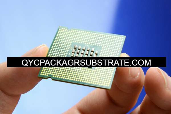
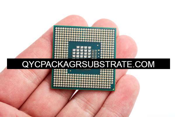
Antenna Shield Package Substrate: This is where SiP intersects with our focus. The antenna shield package substrate provides a platform for the integration of antennas and helps shield electromagnetic interference, ensuring reliable wireless communication.
Significance in Modern Electronics
System in Package (SiP) technology has ushered in an era of innovation, giving rise to smart devices, IoT breakthroughs, wearable gadgets, and cutting-edge automotive systems. Its impact ripples through diverse sectors such as telecommunications, healthcare, automotive, and consumer electronics. SiP’s compact design and exceptional integration capabilities are pivotal in shaping the interconnected landscape we enjoy today, facilitating seamless communication, efficient data processing, and enhanced control. The harmonious interplay of these vital SiP components is revolutionizing how we engage with and derive value from technology in our everyday existence.
The Role of Antenna Shield Package Substrate
Definition of Antenna Shield Package Substrate
In the realm of System in Package (SiP) technology, the antenna shield package substrate serves as a critical component. Essentially, it is a specialized substrate that plays a pivotal role in the functionality and performance of SiP devices. This substrate serves as a foundation for various integrated circuits and components, facilitating their effective integration and performance optimization.
Importance of Shielding in SiP Applications
In SiP applications, the significance of shielding cannot be overstated.
Contemporary electronic devices frequently contend with a barrage of electromagnetic interference (EMI) and radio frequency interference (RFI) emanating from external sources. These interferences have the potential to disrupt signal consistency, diminish operational efficiency, and pose a risk to the device’s functionality.The antenna shield package substrate acts as a safeguard, shielding sensitive components from unwanted interference, ensuring robust signal transmission, and maintaining the overall performance of the SiP system.
Key Features and Requirements
The antenna shield package substrate must possess specific features and meet stringent requirements to fulfill its role effectively. These include:
High Electrical Conductivity: The substrate material must have excellent electrical conductivity to provide a low-resistance path for shielding and grounding, ensuring that EMI and RFI are effectively routed away from the sensitive components.
Compatibility with SiP Components: The substrate must be designed to accommodate the various integrated circuits, passive components, and antennas within the SiP, offering a platform for their secure attachment and interconnection.
Dimensional Stability: Dimensional stability is crucial to ensure that the substrate retains its shape and integrity under varying environmental conditions, safeguarding the SiP’s structural integrity.
Thermal Performance: The substrate material should have good thermal properties to dissipate heat generated within the SiP, preventing overheating and maintaining operational stability.
Customization Options: Antenna shield package substrates often need to be customized to meet the specific requirements of the SiP system, including shape, size, and the placement of openings for antennas.
How it Contributes to Overall SiP Performance
The antenna shield package substrate’s contribution to the overall SiP performance is multifaceted. By providing effective shielding, it mitigates EMI and RFI, ensuring that signals are transmitted and received without interference. This, in turn, results in improved signal integrity and reduced signal loss, optimizing the SiP’s functionality.
Furthermore, the substrate’s ability to house and interconnect various components and antennas in a compact form factor enhances the SiP’s overall efficiency, reducing the footprint and enhancing the integration of multiple functionalities
Material Selection for Antenna Shield Package Substrate
Importance of Material Selection
When it comes to SiP (System in Package) technology, the choice of material for the antenna shield package substrate is of paramount importance. The substrate material plays a critical role in ensuring the overall performance and reliability of the SiP packaging system. Selecting the right material can directly impact signal integrity, thermal management, electromagnetic interference (EMI) shielding, and more.
Common Materials Used in SiP Packaging
SiP packaging substrates are available in various materials, each with its unique properties and advantages. Common materials used in SiP packaging include:
Organic Substrates: Organic substrates, exemplified by materials like FR-4 (Flame Retardant-4), are favored for their cost-effectiveness and manufacturing simplicity. They find common use in applications that demand less stringent performance criteria.
Ceramic Substrates: Ceramic materials, including alumina and aluminum nitride, excel in providing outstanding thermal conductivity and electrical insulation characteristics. They are the material of choice for SiP applications where high performance and efficient heat dissipation are imperative.
Laminate Substrates: Laminate materials, such as polyimide or liquid crystal polymer (LCP), strike a balance between cost and performance. They are suitable for a wide range of SiP applications and are known for their flexibility and low dielectric loss.
Metal Substrates: Metal-based substrates, like copper-invar-copper (CIC) or aluminum nitride metal matrix composites, are used when EMI shielding is a critical requirement. They offer exceptional shielding capabilities and thermal management.
Considerations for Choosing the Right Substrate Material
When selecting the ideal material for an antenna shield package substrate in a SiP system, several key considerations should be taken into account:
Performance Requirements: The specific performance requirements of the SiP, such as signal speed, thermal dissipation, and EMI shielding, should guide material selection.
Cost Constraints: Budget considerations and production volume play a significant role in choosing the right material. Organic substrates may be cost-effective for low-end applications, while ceramics or laminates are preferred for high-performance SiPs.
Environmental Factors: Consider the operating environment, including temperature, humidity, and exposure to harsh chemicals, as these can influence material durability.
Size and Form Factor: The size and form factor of the SiP and the available space for the substrate can limit material choices.
Production Process: Material compatibility with the chosen production processes, such as PCB manufacturing or hybrid integration, is crucial to ensure a successful assembly.
In conclusion, the selection of the antenna shield package substrate material is a pivotal decision in SiP technology, as it directly impacts the SiP’s performance, cost, and durability. By carefully considering the performance requirements, cost constraints, environmental factors, size, and production process compatibility, engineers can make informed choices to optimize the overall SiP system.
Design Considerations
Importance of Proper Design
Design plays a pivotal role in the overall functionality and performance of System in Package (SiP) technology. It’s not just about aesthetics; it’s about ensuring that all components, including the antenna shield package substrate, work seamlessly together to deliver the desired results. Proper design is the foundation upon which a successful SiP system is built.
Design Factors Affecting SiP and Antenna Shield Package Substrate
When it comes to SiP packaging, there are several design factors that need to be taken into account to maximize efficiency and effectiveness:
Component Placement: The strategic positioning of components on the substrate can significantly impact the system’s performance. This includes the location of the antenna shield package and its relationship to other critical components.
Signal Routing: Efficient routing of signals is crucial to maintain signal integrity. The design must ensure minimal interference and crosstalk while also minimizing signal loss.
Thermal Management: Overheating can be detrimental to SiP systems. Adequate heat dissipation mechanisms should be incorporated into the design, and the placement of components should consider thermal considerations.
EMI Shielding: Antenna shield package substrates must be designed to provide effective electromagnetic interference (EMI) shielding. The design should consider the material properties and geometry to enhance EMI protection.
Size and Form Factor: The design should meet the desired form factor and size constraints while accommodating all required components, including the antenna shield package substrate.
Achieving Optimal Signal Integrity and Performance
Achieving optimal signal integrity is at the heart of SiP design. It ensures that the signals are transmitted with minimal distortion and interference, leading to better overall performance.
To achieve this:
Impedance Matching: Proper design should focus on impedance matching, ensuring that signals move seamlessly between components without reflections or signal loss.
Noise Mitigation: Design should incorporate noise reduction techniques, such as signal shielding, proper grounding, and noise filters, to maintain a clean signal path.
Routing and Trace Lengths: Careful consideration of trace lengths and routing paths can minimize signal delays and skew, contributing to better signal integrity.
Isolation and Crosstalk Control: Design should include techniques for isolating sensitive components and controlling crosstalk, reducing interference between different parts of the SiP system.
In summary, SiP design is a critical aspect of optimizing the performance of the technology. It involves various design factors that impact both the SiP system as a whole and the antenna shield package substrate specifically, all with the goal of achieving optimal signal integrity and performance.