
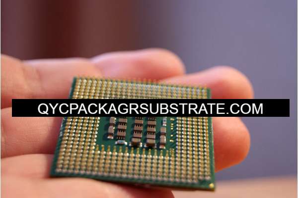
SiP(System in Package) Substrate Manufacturer
SiP(System in Package) Substrate Manufacturer,SiP (System in Package) Substrates are advanced circuit boards designed to integrate multiple semiconductor components into a single package, providing a compact and efficient solution for complex electronic systems. These substrates support the mounting and interconnection of various chips, such as processors, memory, and passive components, within one enclosure. SiP substrates are engineered to handle high-density packaging, offering excellent electrical performance and thermal management. They are ideal for applications where space is limited, such as in smartphones, wearables, and IoT devices. By consolidating multiple functions into a single package, SiP substrates enhance device performance, reduce size, and improve overall reliability.
What is SiP(System in Package) Substrate?
A System in Package (SiP) substrate is an advanced packaging solution used in electronics to integrate multiple semiconductor components into a single package. Unlike traditional integrated circuits (ICs), which combine different functions on a single chip, SiP technology allows for the packaging of diverse components, such as processors, memory, sensors, and passive elements, within one encapsulated unit. This integration enhances functionality, reduces the overall size, and improves performance and reliability.
SiP substrates are designed to support the complex interconnections required for integrating multiple components. They typically feature advanced materials and sophisticated manufacturing processes to accommodate high-density interconnects, fine pitch solder balls, and multiple layers of circuitry. The substrate itself acts as a platform to interconnect these various components, often using technologies such as flip-chip bonding, wire bonding, or through-silicon vias (TSVs) to establish electrical connections.
One of the primary advantages of SiP substrates is their ability to enable compact and efficient designs for consumer electronics, automotive applications, and industrial systems. By consolidating multiple functions into a single package, SiP technology can significantly reduce the footprint of electronic devices and streamline assembly processes. Additionally, SiP substrates can offer improved performance characteristics, such as better signal integrity and thermal management, compared to traditional packaging methods.
Overall, SiP substrates are pivotal in the development of next-generation electronics, supporting increasingly complex and miniaturized devices while meeting the demands for higher performance and integration.
SiP(System in Package) Substrate Manufacturer
What are the SiP(System in Package) Substrate Design Guidelines?
Designing System in Package (SiP) substrates involves several guidelines to ensure optimal performance, reliability, and manufacturability. Here are key design guidelines for SiP substrates:
- Component Layout and Placement: Strategically place components to minimize signal path lengths and enhance performance. High-speed components should be positioned to reduce signal interference and ensure effective heat dissipation. Group related components together to facilitate efficient interconnections.
- Interconnection Design: Use high-density interconnects to manage the complex routing of signals between components. Consider advanced interconnection techniques like flip-chip bonding, wire bonding, or through-silicon vias (TSVs) to achieve high-density and high-speed communication. Ensure that the routing meets the electrical performance requirements and avoids crosstalk.
- Thermal Management: Implement effective thermal management strategies to dissipate heat generated by high-power components. Use thermal vias, heat sinks, and thermal pads to enhance heat dissipation and maintain reliable operation. Conduct thermal simulations to predict and manage temperature profiles.
- Signal Integrity: Maintain signal integrity by carefully designing impedance-controlled traces and minimizing signal degradation. Pay attention to trace lengths, signal routing, and grounding techniques to reduce noise and signal loss. Utilize proper shielding and differential pair routing where necessary.
- Power Distribution: Design robust power distribution networks to ensure stable power delivery to all components. Incorporate multiple power and ground planes to reduce impedance and improve power integrity. Include decoupling capacitors near high-frequency components to stabilize the power supply.
- Manufacturability: Ensure that the substrate design is compatible with the available manufacturing processes and technologies. Design for ease of assembly and testability, including clear pad layouts and appropriate land patterns. Collaborate with manufacturing partners to address any potential issues early in the design phase.
- Mechanical Considerations: Account for mechanical stresses and potential thermal expansion issues in the design. Ensure that the substrate material and design can withstand mechanical forces and thermal cycles without compromising performance or reliability.
- Compliance and Standards: Adhere to industry standards and regulatory requirements for electrical, thermal, and mechanical performance. Ensure that the design meets the specifications for safety, reliability, and environmental considerations.
By following these guidelines, designers can create SiP substrates that support high-performance, reliable, and compact electronic systems, catering to the demands of modern technology applications.
What is the SiP(System in Package) Substrate Fabrication Process?
The fabrication process for System in Package (SiP) substrates involves several critical steps to ensure high performance and reliability of the final product. Here’s an overview of the SiP substrate fabrication process:
- Design and Layout: Begin with detailed design and layout of the SiP substrate, including component placement, interconnections, and thermal management features. Utilize design tools and simulations to optimize the layout for performance and manufacturability.
- Material Preparation: Select and prepare the substrate materials, which typically include organic laminates, ceramics, or advanced composites. The choice of material depends on the required electrical, thermal, and mechanical properties.
- Layer Formation: Fabricate the substrate layers using processes such as lamination for multilayer designs. In cases where ceramic or high-performance materials are used, techniques like tape casting or screen printing may be employed to form the base layers.
- Patterning and Etching: Apply photoresist to the substrate and use photolithography to define the circuit patterns. Expose the photoresist to UV light through a mask, then etch away the unprotected areas to create the desired circuitry and interconnects. This step forms the conductive traces and vias.
- Via Formation: Create vias (vertical electrical connections) through the substrate layers. Techniques such as laser drilling or mechanical drilling are used to form vias, which are then filled with conductive materials like copper to enable inter-layer connections.
- Electroplating and Deposition: Electroplate or deposit metal layers to form the necessary conductive paths and pads. This step ensures the electrical connectivity required for component mounting and signal transmission.
- Component Mounting: Place and attach the electronic components onto the substrate. This can involve techniques such as flip-chip bonding, wire bonding, or ball grid array (BGA) mounting, depending on the design requirements. Ensure precise alignment and secure attachment.
- Encapsulation and Coating: Apply protective encapsulation or coating materials to shield the components and circuitry from environmental factors like moisture and mechanical stress. This step improves the durability and reliability of the SiP.
- Testing and Quality Control: Perform rigorous testing to verify the functionality, performance, and reliability of the SiP substrate. This includes electrical testing, thermal cycling, and mechanical stress testing. Inspect for defects and ensure adherence to design specifications.
- Final Assembly: Conduct any final assembly processes, including trimming, singulation (cutting individual SiP units from the panel), and final packaging. Prepare the SiP substrates for integration into end products.
- Inspection and Verification: Perform a final inspection to ensure that all components are correctly mounted and functioning as intended. Verify that the SiP substrate meets all quality and performance standards before shipping.
By following these steps, manufacturers can produce high-quality SiP substrates that support advanced electronic systems with integrated functions, compact designs, and enhanced performance.
How Do You Manufacture SiP(System in Package) Substrate?
Manufacturing System in Package (SiP) substrates involves a series of specialized processes to ensure high-performance integration of multiple electronic components within a single package. Here’s a detailed overview of the SiP substrate manufacturing process:
- Design and Prototyping: Begin with the design phase, where engineers create detailed schematics and layouts for the SiP substrate. This includes component placement, interconnection routing, and thermal management. Prototype designs are tested and refined to ensure they meet performance requirements.
- Material Selection and Preparation: Choose appropriate substrate materials, which may include organic laminates, ceramics, or advanced composites based on the required electrical, thermal, and mechanical properties. Prepare the materials by cutting them into the required shapes and sizes.
- Layer Fabrication: For multilayer SiP substrates, fabricate the base layers using techniques such as lamination or casting. Each layer is prepared separately, with specific patterns and features designed to accommodate various components and interconnections.
- Patterning and Etching: Apply a photosensitive resist material to the substrate layers. Use photolithography to transfer the circuit patterns onto the substrate. Expose the resist to ultraviolet (UV) light through a mask, and then develop the resist to reveal the underlying substrate material. Etch away the exposed areas to create the desired circuitry and interconnections.
- Via Formation: Drill or laser-cut vias (vertical electrical connections) through the substrate layers. These vias are then filled with conductive materials, such as copper, to establish connections between different layers of the substrate.
- Electroplating and Deposition: Electroplate or deposit metal layers onto the substrate to form the necessary conductive paths and pads. This step involves depositing metals like copper, nickel, or gold to create the electrical connections and surfaces for component mounting.
- Component Integration: Mount electronic components onto the substrate using methods such as flip-chip bonding, wire bonding, or ball grid array (BGA) attachment. Ensure precise alignment and secure attachment of each component to the substrate.
- Encapsulation and Protection: Apply encapsulation materials or protective coatings to shield the substrate and its components from environmental factors such as moisture, dust, and mechanical stress. This improves the durability and reliability of the SiP.
- Testing and Quality Assurance: Conduct thorough testing to verify the functionality and performance of the SiP substrate. This includes electrical testing, thermal cycling, and mechanical stress testing. Inspect for defects and ensure compliance with design specifications and quality standards.
- Final Assembly and Packaging: Perform final assembly steps, such as trimming and singulation (cutting individual SiP units from a larger panel). Package the completed SiP substrates for integration into final electronic products or for further assembly.
- Inspection and Verification: Carry out a final inspection to ensure that all components are properly mounted and that the SiP substrate meets all performance and quality requirements. Verify that the substrate is ready for shipment and integration into end-use applications.
By following these steps, manufacturers can produce high-quality SiP substrates that integrate multiple electronic components into a compact and efficient package, meeting the demands of modern electronic devices and systems.
How Much Should SiP(System in Package) Substrate Cost?
The cost of a System in Package (SiP) substrate can vary significantly based on several factors, including the complexity of the design, the type of materials used, the volume of production, and the specific manufacturing processes employed. Here’s an overview of the factors influencing the cost and a general idea of pricing:
- Design Complexity:SiP substrates with complex designs, such as those incorporating multiple high-density interconnects, advanced packaging technologies, or extensive thermal management features, will generally cost more. The complexity affects the design and manufacturing processes, leading to higher costs.
- Material Selection: The choice of substrate materials impacts cost. High-performance materials like ceramics or advanced organic laminates are more expensive than standard materials. Additionally, the use of specialized materials for thermal or electrical properties will increase costs.
- Production Volume: The cost per unit typically decreases with higher production volumes due to economies of scale. For small-volume or prototype runs, the cost per SiP substrate is higher compared to large-scale production.
- Manufacturing Processes: Advanced manufacturing processes, such as high-density interconnects, fine-pitch bonding, or through-silicon vias (TSVs), add to the cost. The use of state-of-the-art equipment and technologies can increase production costs.
- Component Integration: The number and type of components integrated into the SiP substrate affect the overall cost. SiPs with multiple or high-value components will be more expensive than those with fewer or less costly components.
- Testing and Quality Assurance: Comprehensive testing and quality assurance processes add to the cost. High-quality and reliable SiP substrates require rigorous testing, which impacts the overall price.
These prices are general estimates and can vary widely based on specific requirements and market conditions. For accurate pricing, it is essential to consult with manufacturers who can provide quotes based on detailed design specifications and production needs.
What is SiP(System in Package) Substrate Base Material?
The base material for System in Package (SiP) substrates is crucial in determining the performance, reliability, and overall quality of the final package. Here’s an overview of the typical base materials used for SiP substrates:
- Organic Laminates: Organic laminates are commonly used for SiP substrates due to their flexibility and cost-effectiveness. These materials typically consist of epoxy resins reinforced with fiberglass or other reinforcements. They offer good electrical insulation, reasonable thermal performance, and are suitable for a range of applications. Examples include FR-4, BT (Bismaleimide Triazine), and high-frequency laminates.
- Ceramic Substrates: Ceramic substrates provide excellent thermal conductivity, electrical insulation, and mechanical strength. They are often used in high-power or high-frequency applications where superior performance is required. Common ceramic materials include alumina (Al₂O₃), aluminum nitride (AlN), and beryllium oxide (BeO). These materials are more expensive and harder to process but offer high reliability and stability.
- Polyimide Films: Polyimide is a high-performance polymer used in flexible SiP substrates. It provides excellent thermal stability, electrical insulation, and mechanical flexibility. Polyimide films are often used in applications requiring flexible or conformable substrates, such as in flexible electronics and wearable devices.
- Composite Materials: Composite materials combine various components to achieve desired properties such as enhanced thermal conductivity, reduced weight, or improved mechanical strength. These composites may include combinations of organic and inorganic materials tailored to specific application requirements.
- Build-Up Materials: In advanced SiP designs, build-up layers (also known as build-up films) are used to add additional circuitry and layers on top of a base substrate. These materials, often made of organic polymers, are used in combination with other base materials to create multilayer SiP substrates. They are applied in a process called “build-up” or “layer-by-layer” technology, which involves adding layers of dielectric and conductive materials to achieve complex interconnections.
- High-Frequency Materials: For SiP applications involving high-frequency signals, specialized high-frequency materials are used to ensure signal integrity and reduce losses. These materials often include low-loss ceramics or high-performance organic materials with tailored dielectric properties.
Each of these base materials has its own set of advantages and trade-offs, making the choice of material dependent on the specific requirements of the SiP application, such as electrical performance, thermal management, mechanical properties, and cost considerations.
Which Company Makes SiP(System in Package) Substrate?
There are many companies currently manufacturing System in Package (SiP) substrates in the market. Some notable manufacturers include Intel, TSMC (Taiwan Semiconductor Manufacturing Company), Samsung Electronics, ON Semiconductor, and Hitachi Chemical. These companies have advanced technology and production facilities, capable of providing high-performance SiP substrates widely used in smartphones, communication devices, automotive electronics, and other fields.
Intel, as a global leader in semiconductors, has robust SiP technology and manufacturing capabilities, with SiP products widely used in high-performance computing and consumer electronics. TSMC is renowned for its excellent integrated circuit manufacturing technology, and its SiP solutions support a variety of advanced function integrations. Samsung Electronics, with its strong R&D capabilities in SiP, provides innovative integration solutions. ON Semiconductor focuses on automotive electronics and industrial applications, with SiP substrates performing excellently in these areas. Hitachi Chemical offers highly reliable and high-performance SiP substrates used in consumer electronics and communication devices.
Our company also has the capability to produce System in Package (SiP) substrates. Our SiP substrate products have the following features:
- High Integration: We can integrate multiple functional components into a single SiP substrate, achieving efficient functionality integration suitable for various complex application scenarios.
- Excellent Performance: We use high-performance substrate materials and advanced manufacturing processes to ensure that SiP substrates perform outstandingly in high-frequency and high-speed applications, meeting strict performance requirements.
- Precision Processing: Our company has advanced processing equipment and a skilled technical team capable of high-precision circuit processing and assembly, ensuring product quality and reliability.
- Multi-layer Design:We can design and manufacture multi-layer SiP substrates according to customer needs to support complex circuits and component integration, meeting various application requirements.
- Customized Services: We offer customized SiP substrate design and manufacturing services, providing tailored solutions based on specific customer requirements to ensure that the products fully meet application needs.
- Quality After-Sales Service: We provide comprehensive after-sales service to ensure that customers receive timely technical support and solutions during the usage of our products.
Through continuous technological innovation and strict quality control, our SiP substrates are widely recognized in the market and used in electronic consumer products, communications, automotive electronics, and other fields. If you have a need for SiP substrates, please feel free to contact us. We are committed to providing high-quality products and services.
In summary, whether it is material selection, processing technology, or after-sales service, our company is capable of producing high-quality SiP substrates to meet the needs of various complex electronic systems.
What are the 7 Qualities of Good Customer Service?
Good customer service is crucial for maintaining customer satisfaction and loyalty. Here are seven key qualities that define excellent customer service:
- Responsiveness: Promptness in addressing customer inquiries, concerns, or issues is essential. Good customer service involves quickly acknowledging requests and providing timely solutions, minimizing wait times and frustration.
- Empathy: Understanding and relating to the customer’s feelings and perspective helps build a strong rapport. Empathetic service means listening actively, acknowledging the customer’s emotions, and showing genuine care and concern.
- Effective Communication: Clear, concise, and respectful communication is vital. Good customer service representatives articulate information accurately, use positive language, and ensure that customers understand the solutions or next steps.
- Knowledgeability:Staff should have a thorough understanding of the products, services, and company policies. This expertise allows them to answer questions accurately, resolve issues effectively, and provide useful recommendations.
- Patience: Handling customers with patience, especially in challenging situations, is important. Good customer service representatives remain calm and composed, even when dealing with difficult or repetitive issues, ensuring a positive experience.
- Consistency: Delivering a uniform level of service across all customer interactions is crucial. Consistency in service quality ensures that customers receive the same high standard of care regardless of when or how they engage with the company.
- Problem-Solving Skills: The ability to effectively address and resolve customer issues is a key quality. Good customer service involves not only identifying problems but also finding creative and effective solutions, and following through to ensure complete resolution.
By embodying these qualities, businesses can create positive customer experiences, foster loyalty, and enhance their reputation.
FAQs about SiP(System in Package) Substrate
What is a System in Package (SiP) substrate?
A SiP substrate is a type of electronic packaging that integrates multiple electronic components, such as integrated circuits, passive components, and sensors, into a single package. This approach allows for compact and efficient electronic designs.
What are the benefits of using SiP substrates?
SiP substrates offer several advantages, including reduced size and weight of electronic devices, improved performance through shorter signal paths, lower manufacturing costs due to reduced assembly complexity, and enhanced functionality by integrating diverse components.
What types of materials are used in SiP substrates?
Common materials for SiP substrates include organic laminates (e.g., FR-4, BT resin), ceramics (e.g., alumina, aluminum nitride), polyimide films, and composite materials. The choice of material depends on the performance requirements of the application.
How does SiP compare to traditional packaging methods?
SiP differs from traditional packaging methods by integrating multiple components into a single package rather than using separate packages for each component. This integration can lead to smaller, more efficient designs and can improve electrical performance and thermal management.
What industries use SiP substrates?
SiP substrates are used in various industries, including consumer electronics (smartphones, tablets), automotive (advanced driver assistance systems), telecommunications (base stations, routers), and industrial applications (sensors, control systems).
What are the key design considerations for SiP substrates?
Key considerations include component placement, interconnection design, thermal management, signal integrity, power distribution, and manufacturability. Ensuring these aspects are well-designed is crucial for achieving optimal performance and reliability.