
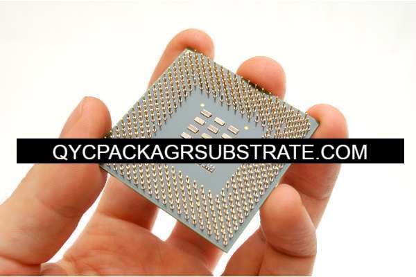
What is SOP Package Substrate?
SOP Package and SOP Package Substrate Vender. we do the SOP package service and we also produce the best samllest bump pitch with 100um, the microtrace with 9um. and the smallest gap are 9um.
SOP (Small Outline Package) substrate is a type of packaging used in semiconductor manufacturing. It refers to the substrate material on which the semiconductor chip is mounted. The SOP package substrate provides electrical connections between the chip and the outside world, as well as mechanical support and protection for the chip.
The SOP package substrate typically consists of several layers of materials, including a base layer made of a dielectric material such as epoxy resin or polyimide, on which conductive traces are patterned using techniques like lithography and etching. These traces form the electrical pathways that connect the chip’s bond pads to the package’s external pins or leads.
In addition to the conductive traces, the SOP package substrate may also include other components such as vias (vertical interconnect access) for connecting traces on different layers, solder mask for protecting the traces and preventing short circuits, and solder balls or pads for attaching the package to the circuit board.
SOP package substrates come in various sizes and configurations to accommodate different chip sizes and pin counts. They are commonly used in consumer electronics devices such as smartphones, tablets, and laptops, where space is limited and low cost is important.
SOP Package Substrate
What are the functions of SOP Package Substrate?
The functions of SOP Package Substrate include:
Providing electrical connections: SOP Package Substrate connects the chip’s bond pads to the external pins or leads of the package through conductive pathways, thereby establishing electrical connections between the chip and external circuits.
Providing mechanical support and protection: SOP Package Substrate offers physical support and protection to the chip, preventing mechanical damage or environmental effects such as vibration, shock, moisture, and dust.
Heat dissipation: SOP Package Substrate helps to conduct the heat generated by the chip to the package’s exterior, maintaining the chip’s operating temperature within normal limits and preventing overheating.
Supporting packaging processes: SOP Package Substrate supports packaging processes such as printing, plating, soldering, and testing, facilitating the achievement of high-quality and efficient packaging.
Overall, SOP Package Substrate plays a crucial role in semiconductor device packaging by providing electrical connections and mechanical support, aiding in heat management, and supporting packaging processes.
What are the different types of SOP Package Substrate?
There are several different types of SOP (Small Outline Package) substrates commonly used in semiconductor packaging. Some of the most common types include:
Printed Circuit Board (PCB) Substrates: These substrates are made of layers of fiberglass or other insulating materials with copper traces patterned on them. They are commonly used in SOP packages for their versatility and ability to support complex circuitry.
Leadframe Substrates: Leadframe substrates are typically made of a metal alloy such as copper or copper alloy. They consist of a grid-like structure with leads extending outward from the edges. Leadframe substrates are often used in SOP packages for their cost-effectiveness and ease of manufacturing.
Ceramic Substrates: Ceramic substrates are made of materials such as alumina (aluminum oxide) or aluminum nitride. They offer excellent thermal conductivity and mechanical strength, making them suitable for high-power applications where heat dissipation is critical.
Organic Substrates: Organic substrates are made of organic materials such as epoxy resin or polyimide. They are lightweight, flexible, and cost-effective, making them suitable for small form factor applications such as mobile devices and consumer electronics.
Silicon Substrates: Silicon substrates are made of single-crystal silicon wafers. They offer high thermal conductivity and compatibility with semiconductor processes, making them suitable for high-performance applications such as RF (radio frequency) and microwave devices.
These are just a few examples of the different types of SOP package substrates available. The choice of substrate depends on factors such as cost, performance requirements, and the specific needs of the application.
What is the relationship between SOP Package Substrate and IC packaging?
The SOP (Small Outline Package) substrate is an integral part of IC (Integrated Circuit) packaging. IC packaging refers to the process of enclosing one or more semiconductor chips (ICs) in a protective housing or package, which provides electrical connections, mechanical support, and protection for the chip. The SOP package substrate serves as the foundation upon which the semiconductor chip is mounted and connected to the external leads or pins of the package.
The relationship between SOP package substrate and IC packaging can be understood in the following ways:
Electrical connections: The SOP package substrate provides the electrical pathways for connecting the bond pads on the semiconductor chip to the external leads or pins of the package. These pathways are typically made of conductive traces patterned on the substrate material, allowing for the transmission of electrical signals between the chip and the outside world.
Mechanical support and protection: The SOP package substrate offers physical support and protection for the semiconductor chip, preventing mechanical damage and environmental effects such as vibration, shock, moisture, and dust. It also helps to dissipate heat generated by the chip, thereby maintaining the chip’s operating temperature within normal limits.
Compatibility with packaging processes: The SOP package substrate must be compatible with various packaging processes, including printing, plating, soldering, and testing. It serves as a platform for these processes and facilitates the assembly of the semiconductor chip into the final package.
In summary, the SOP package substrate is an essential component of IC packaging, providing electrical connections, mechanical support, and compatibility with packaging processes. It plays a crucial role in protecting and enhancing the performance of semiconductor chips in a wide range of applications.
How does SOP Package Substrate differ from PCB?
SOP (Small Outline Package) substrate and PCB (Printed Circuit Board) are both types of substrates used in electronics manufacturing, but they serve different purposes and have distinct characteristics. Here are some key differences between SOP Package Substrate and PCB:
Function:
SOP Package Substrate: The primary function of SOP package substrate is to provide electrical connections between the semiconductor chip and the external leads or pins of the package. It also offers mechanical support and heat dissipation for the chip.
PCB: PCB serves as a platform for mounting and interconnecting electronic components such as resistors, capacitors, and integrated circuits. It provides electrical connections between components and supports the overall functionality of the electronic device.
Composition:
SOP Package Substrate: SOP package substrates are typically made of materials such as fiberglass, ceramic, or organic substrates. They often feature conductive traces patterned on the substrate material to facilitate electrical connections.
PCB: PCBs are typically made of layers of fiberglass or other insulating materials with copper traces patterned on them. These traces form the electrical pathways that connect the various components mounted on the PCB.
Application:
SOP Package Substrate: SOP package substrates are specifically designed for use in semiconductor packaging, where they serve as the foundation for mounting and connecting semiconductor chips in packages such as SOP, QFN (Quad Flat No-Lead), and BGA (Ball Grid Array).
PCB: PCBs are used in a wide range of electronic devices and applications, including computers, smartphones, televisions, automotive electronics, and industrial equipment.
Complexity:
SOP Package Substrate: SOP package substrates are typically simpler in design compared to PCBs, as they are specifically tailored to the requirements of semiconductor packaging.
PCB: PCBs can vary significantly in complexity, depending on the specific application and design requirements. They can feature multiple layers, complex routing, and a variety of components mounted on both sides of the board.
In summary, while both SOP Package Substrate and PCB are substrates used in electronics manufacturing, they have different functions, compositions, applications, and levels of complexity. SOP package substrates are specialized for semiconductor packaging, while PCBs are used in a wide range of electronic devices and applications.
What are the structure and production technology of SOP Package Substrate?
The structure and production technology of SOP (Small Outline Package) Package Substrate can vary depending on factors such as the type of substrate material used and the specific requirements of the application. However, here is a general overview of the structure and production technology of SOP Package Substrate:
Structure:
Substrate Material: SOP Package Substrates are typically made of materials such as fiberglass, ceramic, organic substrates (e.g., epoxy resin or polyimide), or metal alloys (e.g., copper or copper alloy). The choice of substrate material depends on factors such as cost, thermal performance, and electrical properties.
Conductive Traces: SOP Package Substrates feature conductive traces patterned on the substrate material using techniques such as lithography and etching. These traces form the electrical pathways that connect the semiconductor chip’s bond pads to the external leads or pins of the package.
Vias: Vias are small holes drilled or etched into the substrate material, allowing conductive traces to pass between different layers of the substrate. Vias are used to create multi-layered substrates and facilitate the routing of electrical connections.
Solder Mask: Solder mask is a protective layer applied to the substrate surface to insulate the conductive traces and prevent short circuits during soldering. It is typically made of a polymer material such as epoxy or solder resist ink.
Production Technology:
Substrate Fabrication: The production process begins with the fabrication of the substrate material, which involves processes such as mixing, pressing, and curing (for organic substrates), or sintering (for ceramic substrates).
Conductive Traces Patterning: Next, conductive traces are patterned on the substrate material using lithography and etching techniques. A photosensitive material is applied to the substrate surface, exposed to UV light through a mask, and then developed to remove the unwanted areas. The exposed substrate is then etched to remove the unmasked material, leaving behind the conductive traces.
Via Formation: Vias are formed by drilling or etching small holes into the substrate material. These vias are then filled with a conductive material such as copper or plated with metal to create electrical connections between different layers of the substrate.
Solder Mask Application: Solder mask is applied to the substrate surface using screen printing or inkjet printing techniques. The solder mask is cured to form a protective layer over the conductive traces, leaving only the areas where soldering is required exposed.
Surface Finish: Finally, the substrate surface may undergo surface finishing processes such as hot air solder leveling (HASL), electroless nickel immersion gold (ENIG), or organic solderability preservatives (OSP) to improve solderability and corrosion resistance.
Overall, the production technology of SOP Package Substrate involves a series of fabrication and patterning processes to create the substrate structure and electrical connections required for semiconductor packaging.
Frequently Asked Questions (FAQs)
What is SOP Package Substrate?
SOP Package Substrate refers to the material used as the foundation for mounting and connecting semiconductor chips in Small Outline Package (SOP) packages. It provides electrical connections, mechanical support, and protection for the chip.
What are the functions of SOP Package Substrate?
The functions of SOP Package Substrate include providing electrical connections between the semiconductor chip and the package leads, offering mechanical support and protection for the chip, facilitating heat dissipation, and supporting packaging processes.
How does SOP Package Substrate differ from PCB?
While both SOP Package Substrate and PCB (Printed Circuit Board) are substrates used in electronics manufacturing, they serve different purposes. SOP Package Substrate is specifically designed for semiconductor packaging, providing electrical connections and mechanical support for the chip. PCB, on the other hand, is used to mount and interconnect electronic components in various electronic devices.
What is the relationship between SOP Package Substrate and IC packaging?
SOP Package Substrate is an integral part of IC (Integrated Circuit) packaging. It provides the foundation for mounting and connecting semiconductor chips in packages such as SOP, QFN (Quad Flat No-Lead), and BGA (Ball Grid Array), thereby facilitating electrical connections, mechanical support, and protection for the chip.
What are the different types of SOP Package Substrate?
Common types of SOP Package Substrate include Printed Circuit Board (PCB) Substrates, Leadframe Substrates, Ceramic Substrates, Organic Substrates, and Silicon Substrates. Each type has its own characteristics and is used in different applications based on factors such as cost, performance requirements, and thermal properties.
What is the structure and production technology of SOP Package Substrate?
The structure of SOP Package Substrate typically includes substrate material, conductive traces, vias, and solder mask. The production technology involves processes such as substrate fabrication, conductive traces patterning, via formation, solder mask application, and surface finishing to create the substrate structure and electrical connections required for semiconductor packaging.
Conclusion
In conclusion, SOP Package Substrate plays a critical role in semiconductor packaging by providing essential functions such as electrical connections, mechanical support, and protection for semiconductor chips. It serves as the foundation upon which semiconductor chips are mounted and connected to the external leads or pins of the package. SOP Package Substrate differs from PCB in its specific application and design, tailored for semiconductor packaging rather than general electronic component interconnection. Understanding the relationship between SOP Package Substrate and IC packaging is crucial for ensuring the reliability and performance of semiconductor devices. Additionally, there are various types of SOP Package Substrate available, each with its unique characteristics and applications. The structure and production technology of SOP Package Substrate involve a series of fabrication and patterning processes to create the substrate’s structure and electrical connections required for semiconductor packaging. Overall, SOP Package Substrate contributes significantly to the functionality, performance, and reliability of semiconductor devices in a wide range of applications.