
We are a professional packaging substrate supplier, we mainly produce ultra-small bump pitch substrate, ultra-small trace and spacing packaging substrate and PCBs.In today’s rapidly evolving technological landscape, substrate packaging stands as a pivotal enabler, facilitating the seamless integration of intricate electronic components within a myriad of devices. As the backbone of modern electronics, substrate packaging forms the very foundation upon which our interconnected world operates. From the miniature circuits in our smartphones to the intricate systems in automobiles, substrate packaging plays an indispensable role in ensuring the functionality and durability of electronic products.
The development of substrate packaging technology
At the heart of this discourse lies an exploration of the dynamic evolution of substrate packaging technology. Delving into its historical roots, this article aims to unravel the transformative journey that substrate packaging has undertaken, from its conventional manifestations to the cutting-edge innovations defining its contemporary landscape. By delving into the various advancements and trends shaping the field, we seek to shed light on the significant strides that have propelled substrate packaging to the forefront of modern engineering.
Fundamentals of Substrate Packaging Technology
Defining Substrate Packaging and Its Role
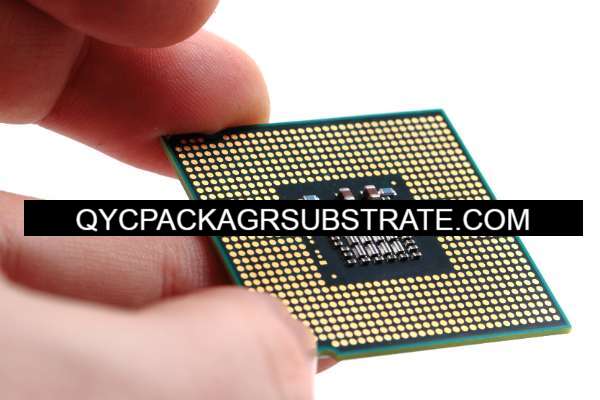
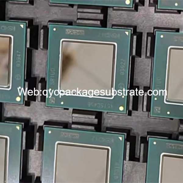
Substrate packaging technology, at its core, refers to the process of encapsulating and connecting integrated circuits within a protective housing or substrate. It acts as a bridge between the integrated circuits and the external environment, ensuring the integrity and functionality of electronic devices. This packaging serves as the protective shell for the delicate electronic components, safeguarding them from physical damage, environmental factors, and electromagnetic interference.
The role of substrate packaging can be likened to the protective casing of a precious gem. Just as a gem’s setting enhances its beauty and shields it from harm, substrate packaging plays a vital role in safeguarding and enhancing the performance of integrated circuits. It not only provides physical protection but also facilitates electrical connections and thermal management, making it an integral part of modern electronics.
The Critical Importance of Substrate Packaging in the Electronics Industry
Substrate packaging is undeniably a linchpin in the world of electronics. Its significance can be observed through its impact on various aspects of the industry:
1.Miniaturization: As the demand for smaller and more compact electronic devices grows, substrate packaging technology enables the assembly of tiny yet highly functional components. This miniaturization trend has revolutionized the way we use and interact with electronics, from smartphones to wearable devices.
2.Performance Enhancement: Modern electronic gadgets are expected to deliver ever-increasing performance. Substrate packaging plays a crucial role in dissipating heat efficiently, ensuring that electronic components can operate at peak performance without overheating.
3.Reliability: The reliability of electronic devices depends on their ability to withstand environmental stresses, mechanical shocks, and temperature variations. Substrate packaging ensures the durability and long-term functionality of electronic products, even in harsh conditions.
4.Interconnectivity: The electronics industry relies on seamless communication between different components. Substrate packaging not only protects integrated circuits but also facilitates the intricate network of connections that allow devices to function as cohesive systems.
In summary, the role of substrate packaging is indispensable. It acts as the guardian of the electronic world, ensuring that the heart of every electronic device
Evolution of Substrate Packaging
A Brief Overview of Traditional Packaging Techniques
In the not-so-distant past, traditional substrate packaging techniques dominated the electronics industry. These methods primarily revolved around Dual In-line Packages (DIPs) and other through-hole technologies. DIPs involved mounting electronic components on a flat circuit board with pins extending through the board, soldered on the reverse side. While effective in their time, traditional packaging techniques had their limitations. They were bulkier, less efficient in terms of space utilization, and less suitable for the miniaturization trend.
These techniques struggled to keep pace with the ever-increasing demand for smaller, more efficient electronic devices. Manufacturers sought a solution to this problem, leading to the evolution of modern substrate packaging technologies.
The Demand for Modern Substrate Packaging Technologies
As consumer expectations for electronics continued to evolve, there was an increasing demand for smaller, lighter, and more powerful devices. Smartphones, wearables, and IoT devices needed to be compact yet packed with cutting-edge capabilities. Traditional packaging techniques couldn’t meet these demands.
This growing demand served as the catalyst for the development of modern substrate packaging technologies. The industry realized the need for innovation to overcome the limitations of traditional packaging. In response, new approaches, such as System-in-Package (SiP) and Chip-on-Board (COB) emerged. These technologies allowed for smaller form factors, better thermal management, and increased electrical performance.
Moreover, the demand for greater functionality and connectivity in electronics also drove the evolution of substrate packaging. Consumers wanted devices with more features and seamless integration, requiring intricate designs and advanced interconnectivity. The transition to modern substrate packaging technologies allowed for the integration of multiple functions within a single package, providing the foundation for the smart devices we use today.
In summary, the shift from traditional to modern substrate packaging techniques was driven by the need for smaller, more powerful, and highly integrated electronic products. This transition not only met consumer demands but also paved the way for the current era of compact, high-performance electronics.
A Fresh Perspective on Substrate Packaging
We will delve into a fresh perspective on substrate packaging, which emphasizes sustainability and eco-friendliness, while also exploring the exciting future trends in this critical technology.
Emphasizing Sustainability and Eco-Friendliness
As the global focus on environmental sustainability continues to grow, the electronics industry, including substrate packaging, is under increasing pressure to reduce its environmental footprint. Traditional packaging methods have often relied on materials and processes that generate waste and contribute to pollution. In contrast, modern substrate packaging is embracing eco-friendly practices.
With a commitment to sustainability, substrate packaging is now utilizing materials that are not only efficient but also environmentally responsible. Eco-friendly substrates, for instance, are gaining prominence due to their reduced carbon footprint and recyclability. These substrates can minimize electronic waste and contribute to a cleaner, greener industry.
Furthermore, the development of energy-efficient packaging processes and the optimization of resource use have become central to the substrate packaging landscape. By minimizing energy consumption and waste production, this shift not only benefits the environment but also aligns with cost-saving objectives, making it a win-win for manufacturers and consumers alike.
Exploring the Future Trends in Substrate Packaging
The future of substrate packaging is poised for exciting developments that go beyond the conventional. With the rapid evolution of technology, several promising trends are emerging:
1.Miniaturization and Enhanced Performance: The demand for smaller, yet more powerful electronic devices is pushing substrate packaging towards miniaturization. Advanced packaging solutions are being developed to accommodate smaller form factors while increasing performance and functionality.
2.Advanced Materials: Innovations in materials, including flexible substrates and organic semiconductors, are opening new avenues for substrate packaging. These materials offer enhanced flexibility, reduced weight, and the potential for sustainable, biodegradable options.
3.High-Density Interconnects: High-density interconnects, such as micro vias and 3D packaging, are enabling faster data transfer rates and improved signal integrity. This trend is crucial in meeting the growing demands of high-speed computing and 5G technology.
4.Integration of AI and IoT: Substrate packaging is increasingly incorporating Artificial Intelligence (AI) and Internet of Things (IoT) elements. These technologies enable smart packaging solutions that can monitor and adapt to their environment, providing improved functionality and user experience.
5.Energy Efficiency: Future substrate packaging will focus on enhancing energy efficiency, extending battery life, and reducing power consumption. This trend is particularly important as we look to reduce our overall energy consumption.
In conclusion, the substrate packaging landscape is undergoing a transformation, with a strong emphasis on sustainability and an exciting array of future trends. By adopting eco-friendly practices and exploring new technologies, the electronics industry is not only meeting the demands of today but also positioning itself for a more environmentally responsible and innovative future. Substrate packaging is no longer just about protecting electronic components; it’s about shaping a more sustainable and technologically advanced world.