
We are a professional substrate semiconductor packaging supplier, we mainly produce ultra-small bump pitch semiconductor package substrates from 4 layer to 20 layers.
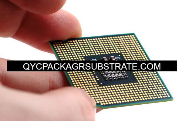
A substrate in semiconductor packaging serves as the foundational platform for electronic components, connecting and supporting various elements of the semiconductor device. Understanding its significance is essential in the realm of semiconductor technology. Let’s delve into this crucial aspect:
Definition and Basic Functions
The primary functions of a substrate include:
Electrical Connectivity: Substrates facilitate the connection of the semiconductor device to external circuitry, enabling data transfer and power distribution.
Heat Dissipation: They assist in managing the heat generated during semiconductor operation, preventing overheating and ensuring optimal performance.
Mechanical Support: Substrates offer structural support and protection to the fragile semiconductor chip, safeguarding it from physical damage.
Types of Substrates Used in Semiconductor
Packaging Substrates come in various forms to suit different applications.
Common Materials Used in Substrate Manufacturing
The choice of substrate material plays a critical role in semiconductor packaging. Here are some common materials employed in substrate manufacturing:
FR-4: FR-4 substrates, composed of an epoxy resin and woven glass fabric, are cost-effective and widely used in various electronics applications. Their affordability and ease of fabrication make them a popular choice for simple printed circuit boards (PCBs) and some semiconductor packages.
Ceramic: Ceramic substrates provide superior thermal management and mechanical strength. They are widely used in power modules, RF (Radio Frequency) devices, and applications that demand efficient heat dissipation.
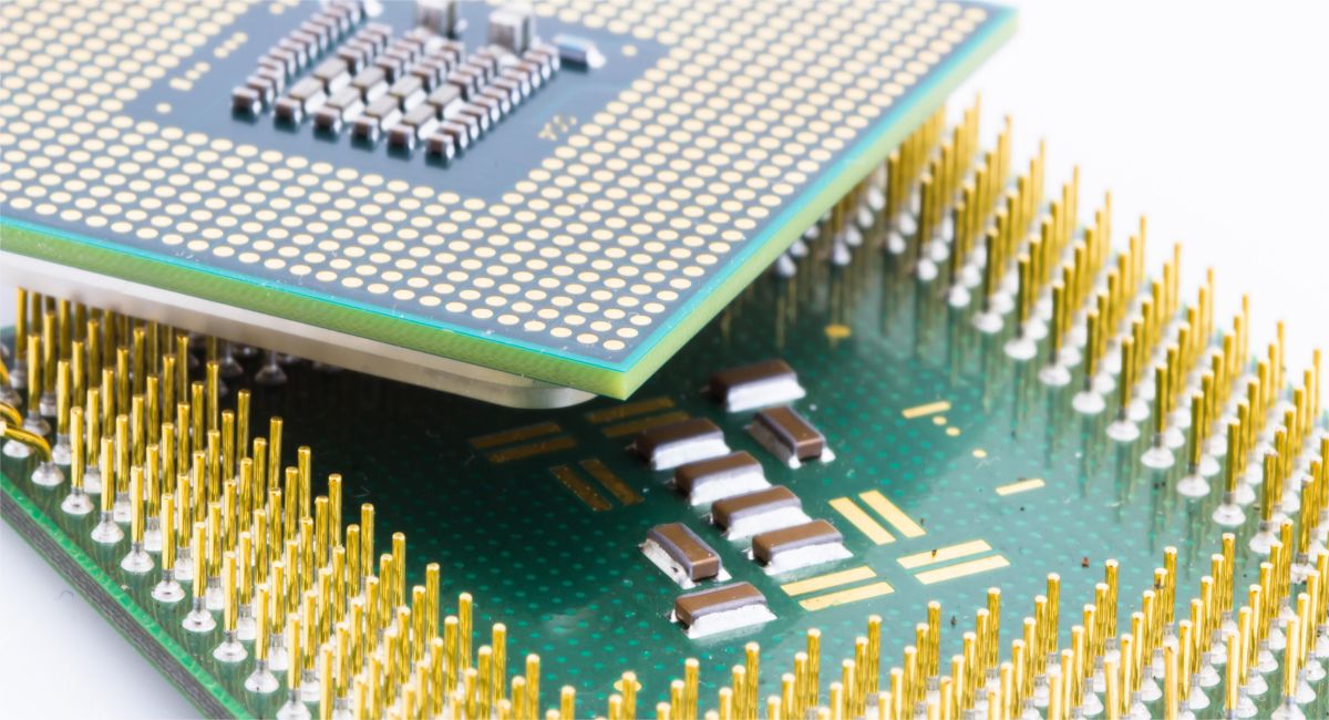
Substrates are a linchpin in the semiconductor packaging process. They serve as the bridge connecting the semiconductor die or chip to the external world. By providing structural support, enabling electrical connections, and managing heat, substrates contribute significantly to the functionality, reliability, and performance of semiconductor devices. As technology advances, the choice of substrate and its design continue to be critical factors in achieving optimal semiconductor packaging solutions.
Why Substrates Matter
Substrates play a pivotal role in semiconductor packaging, influencing various critical aspects of semiconductor performance and reliability. Understanding why substrates matter is essential, and it can be broken down into the following key factors, each of which aligns with the broader theme of semiconductor packaging:
Electrical Considerations
Signal Transmission: The choice of substrate material and design can significantly impact signal quality, ensuring that data and power transmission occur with minimal loss or interference. This is especially crucial in high-speed and high-frequency applications, where even slight disruptions can lead to performance issues.
Thermal Properties: Heat management is a critical aspect of semiconductor operation.
Mechanical Considerations
Support and Protection for the Semiconductor Device: Substrates provide physical support and protection to the delicate semiconductor device. They act as a structural foundation, safeguarding the semiconductor from mechanical stresses, shocks, and vibrations. A well-designed substrate ensures the device remains intact and operational under various environmental conditions, increasing its longevity and robustness.
Integration with Other Packaging Components: Semiconductor packaging is a complex ecosystem where different components work in unison. Substrates must seamlessly integrate with other packaging elements, such as solder balls, interconnects, and encapsulation materials. Their mechanical properties, such as rigidity and coefficient of thermal expansion (CTE), need to be carefully matched to avoid stress-induced failures and ensure the overall package’s structural integrity.
Impact on Semiconductor Performance and Reliability
The collective influence of electrical and mechanical considerations ultimately determines the semiconductor’s performance and reliability. Substrates that excel in facilitating signal transmission and thermal management contribute to efficient and dependable semiconductor operation. Conversely, poor substrate choices can lead to signal degradation, thermal issues, and even premature semiconductor failure. The reliability of the entire semiconductor package hinges on the substrate’s ability to maintain optimal conditions for the semiconductor device.
In summary, substrates are the unsung heroes of semiconductor packaging, silently shaping the performance and reliability of the technology that powers our modern world. By addressing these electrical and mechanical considerations, substrate selection and design become critical factors in ensuring the success of semiconductor devices across a wide range of applications.
Substrate Manufacturing
Substrate Fabrication Process
When it comes to manufacturing substrates for semiconductor packaging, a precise and controlled process is essential to ensure the quality and performance of the final product. The substrate fabrication process involves several key steps:
Material Selection: The choice of substrate material is crucial, as it directly impacts the electrical, thermal, and mechanical properties of the semiconductor package. Common materials include FR-4, silicon, and ceramics. Each material has its unique characteristics and manufacturing requirements.
Lamination: In the case of organic substrates like FR-4, a lamination process is used. Layers of material are bonded together using heat and pressure to create a solid substrate with the desired thickness. This process ensures the substrate’s structural integrity.
Circuit Formation: Substrates often include printed circuit patterns, which are created using processes like photolithography, etching, and plating. These circuits are essential for routing signals within the semiconductor package.
Dielectric Layer Application: Insulating dielectric layers are applied to isolate conductive traces and components, preventing short circuits and ensuring signal integrity.
Via Formation: Vias are small holes drilled or etched into the substrate to allow for interconnection between different layers. Vias are a critical element in multilayer substrates.
Surface Finish: The substrate’s surface finish is vital for ensuring good solderability and electrical connections with semiconductor devices. Common finishes include solder mask, ENIG (Electroless Nickel Immersion Gold), and OSP (Organic Solderability Preservatives).
Key Parameters in Substrate
Manufacturing Several key parameters must be closely monitored during the substrate manufacturing process to achieve the desired performance and reliability:
Dielectric Constant (Dk): This parameter characterizes the material’s ability to store electrical energy and affects signal propagation speed. A low Dk is typically preferred for high-speed applications.
Dimensional Stability: Substrates must maintain their shape and dimensions under various environmental conditions. Dimensional stability ensures proper alignment and connection of components.
Copper Thickness and Roughness: The thickness and surface roughness of copper traces and vias impact electrical performance and reliability. Precise control is essential.
Registration Accuracy: This parameter refers to the alignment of different layers and features on the substrate. High registration accuracy is necessary to ensure proper interconnection and signal routing.
Advances in Substrate Manufacturing Technology
As technology continues to advance, substrate manufacturing processes have also seen significant improvements. Some noteworthy advancements include:
Miniaturization: Substrates are being manufactured with smaller feature sizes to accommodate the demands of miniaturized electronic devices. Advanced lithography techniques enable the creation of finer circuit patterns and smaller vias.
Multilayer Substrates: To support complex semiconductor packages, multilayer substrates are becoming more common. Advanced manufacturing techniques allow for the creation of intricate multilayer structures, enhancing signal routing and reducing the footprint.
3D Packaging: Substrates are now designed to support three-dimensional packaging configurations, enabling improved thermal management and integration of multiple semiconductor devices within a single package.
Substrate Selection for Different Applications
Choosing the Right Substrate Material for Specific Applications
In the world of semiconductor packaging, the choice of substrate material is far from one-size-fits-all. It’s crucial to carefully consider the specific application, as different applications demand different substrate characteristics. Let’s delve into how the right substrate material can make all the difference:
Consumer Electronics: For lightweight and cost-effective devices like smartphones and tablets, organic substrates like FR-4 are often preferred due to their low cost and excellent electrical insulation properties.
High-Performance Computing: In applications that require high-speed data processing, inorganic substrates such as silicon or advanced ceramics may be favored. These materials have superior thermal conductivity, making them ideal for dissipating heat in powerful processors.
Automotive Electronics: Vehicles demand robust and reliable electronics. Substrates that can withstand wide temperature ranges and mechanical stress are essential. This often leads to the use of ceramic substrates.
Trade-Offs and Considerations in Substrate Selection
When selecting a substrate, engineers must navigate trade-offs to find the optimal solution. Several factors come into play:
1.Cost vs. Performance: Organic substrates like FR-4 are cost-effective, but they may not meet the performance requirements of high-end applications. Engineers must balance cost considerations with performance needs.
2.Thermal Management: In applications where heat dissipation is crucial, the substrate’s thermal conductivity becomes a paramount consideration. Silicon and ceramics excel in this regard but may be more expensive.
3.Form Factor: The size and shape of the semiconductor device also influence substrate choice. Smaller, compact devices may lean towards organic substrates, while larger systems may opt for inorganic options.
4.Environmental Factors: Harsh environmental conditions, such as extreme temperatures or exposure to chemicals, impact substrate selection. Some substrates are better suited for withstanding such conditions.
Case Studies Highlighting Substrate Selection in Real-World Applications
Real-world applications offer insightful examples of substrate selection:
Space Exploration: In the aerospace industry, where reliability and extreme conditions are paramount, ceramic substrates are often chosen for their resilience. The Mars rovers, for instance, use ceramic substrates to endure the planet’s harsh environment.
5G Infrastructure: The rapid expansion of 5G networks demands high-performance electronics. Many base stations use silicon substrates to manage the heat generated by intense data processing.
Medical Devices: In medical applications, where compact size, reliability, and biocompatibility are essential, substrate materials such as silicon play a crucial role in manufacturing cutting-edge medical devices.
By examining these case studies, it becomes evident that substrate selection is a critical decision that directly influences the functionality, reliability, and cost-effectiveness of semiconductor devices across various industries. The right substrate material can be the linchpin of success in any given application, making it a central consideration for engineers and manufacturers alike.
Substrate Trends and Innovations
Emerging Trends in Substrate Technology
In the dynamic field of semiconductor packaging, substrates are constantly evolving to meet the growing demands for performance, miniaturization, and energy efficiency. Several emerging trends in substrate technology have garnered attention:
Embedded Passive Components: Substrates are now being engineered to integrate passive components like resistors and capacitors directly into the substrate material. This trend reduces the footprint of electronic devices, enhancing miniaturization.
3D Packaging: As the semiconductor industry pushes the boundaries of miniaturization, 3D packaging has gained prominence. Advanced substrates are being developed to support the vertical stacking of chips, reducing interconnect lengths and improving overall system performance.
Flexible and Stretchable Substrates: The rise of flexible and wearable electronics has spurred innovation in substrates that can bend and stretch without compromising electrical performance. These substrates open doors to new applications, such as flexible displays and healthcare devices.
The Role of Substrates in Advanced Packaging Techniques
In modern semiconductor packaging, substrates play a pivotal role in advanced packaging techniques:
System-in-Package (SiP): SiP is an increasingly popular approach that integrates multiple semiconductor dies, passive components, and even MEMS devices into a single package. Substrates are the structural backbone for these complex packages, providing interconnections and support for various components.
Fan-Out Wafer-Level Packaging (FOWLP): FOWLP leverages advanced substrates to create highly compact and power-efficient packages. By redistributing I/Os across the package surface, FOWLP enhances the electrical and thermal performance of semiconductor devices.
Through-Silicon Via (TSV): TSV technology, often used in 3D packaging, relies on substrates with embedded vias to establish vertical connections between stacked chips. Substrates with precisely engineered TSVs are vital for optimizing signal integrity and heat dissipation in these packages.
Sustainability and Environmental Considerations in Substrate Manufacturing
As the semiconductor industry continues to expand, it’s crucial to address sustainability and environmental concerns in substrate manufacturing:
Materials Recycling: To reduce waste and environmental impact, manufacturers are exploring recycling and repurposing of substrate materials. This approach aligns with sustainability goals and minimizes the carbon footprint of semiconductor packaging.
Eco-Friendly Substrate Materials: There is a growing interest in developing substrates from eco-friendly and biodegradable materials. These materials aim to reduce the environmental impact of semiconductor packaging, especially in disposable consumer electronics.
Energy-Efficient Manufacturing: Substrate manufacturers are implementing more energy-efficient production processes, such as adopting renewable energy sources and optimizing resource usage. This not only reduces costs but also lowers the industry’s carbon emissions.
In conclusion, the world of substrate technology is witnessing a transformative phase, with emerging trends, advanced packaging techniques, and a growing emphasis on sustainability. These developments are reshaping the semiconductor packaging landscape, promising more compact, efficient, and environmentally responsible electronic devices in the future. Understanding these trends is essential for staying at the forefront of the semiconductor industry.