
What is Ultra-small gap high speed PCB?
Ultra-small gap high speed PCB supplier. High speed and high frequency material packaging substrate manufacturing. Advanced Msap and Sap packaging substrate production process and technology.
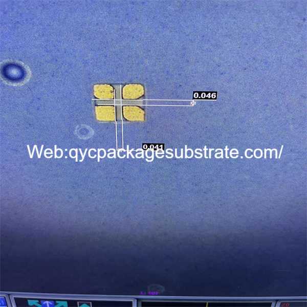
An “Ultra-small gap high-speed PCB” typically refers to a printed circuit board (PCB) that is designed with very narrow gaps between the conductive traces or lines on the board. This type of PCB is often used in high-speed electronic devices and systems where signal integrity and transmission speed are critical.
Here are key features and considerations associated with ultra-small gap high-speed PCBs:
Small Gap Design: The term “ultra-small gap” implies that the spacing between adjacent traces or conductive elements on the PCB is minimized. In high-frequency scenarios, minimizing signal interference, crosstalk, and ensuring precise signal transmission are essential considerations.
High-speed PCBs find common applications in electronic systems that function at elevated frequencies, including telecommunications, data communication, high-speed computing, and various scenarios requiring swift and dependable signal transmission.
Signal Integrity:Preserving signal integrity stands as a foremost consideration in the design of high-speed PCBs.The small gaps help to minimize signal distortion and other issues that can arise at higher frequencies.
Impedance Control: Ultra-small gap high-speed PCBs often require precise impedance control to match the characteristic impedance of transmission lines. This is important for preventing signal reflections and ensuring efficient signal propagation.
Material Selection: The choice of PCB materials is critical for high-speed applications. Materials with low dielectric constant and low loss tangent are often preferred to minimize signal attenuation.
Advanced Manufacturing Techniques:
Manufacturing ultra-small gap high-speed PCBs may incorporate sophisticated methods like fine-pitch surface mount technology (SMT), controlled impedance routing, and precise etching processes.
Electromagnetic Interference (EMI) Mitigation:In high-speed scenarios, managing electromagnetic interference (EMI) becomes a significant consideration. Design strategies, including component placement and the application of shielding techniques, can be employed to mitigate EMI.
Testing and Validation:Given the crucial role of signal integrity in high-speed applications, comprehensive testing and validation become imperative. This may involve using specialized equipment to measure signal characteristics and ensure compliance with industry standards.
In summary, an ultra-small gap high-speed PCB is designed to meet the demanding requirements of high-frequency electronic systems, with a focus on minimizing signal degradation, maintaining signal integrity, and ensuring reliable performance.
What Drives the Evolution of Ultra-Small Gap High-Speed PCBs?
In the dynamic realm of electronics, several factors drive the evolution of ultra-small gap high-speed PCBs (Printed Circuit Boards). These factors include:
The continuous progress in communication, computing, and embedded systems has generated a growing requirement for smaller dimensions and increased speeds in electronic componentsTechnological advancements in areas like 5G communication, Internet of Things (IoT) devices, and high-performance computing have elevated the standards for both the dimensions and operational capabilities of circuit boards.
Enhancing performance is vital in electronic devices, particularly in mobile devices and computer systems where achieving high-speed functionality is essential.The development of ultra-small gap high-speed PCBs contributes to this objective by providing shorter signal transmission paths, minimizing signal latency, and achieving elevated data transfer rates. These advancements collectively enhance the overall system performance.
As electronic devices advance, there is a corresponding surge in the demand for efficient power consumption and heat dissipation. The adoption of ultra-small gap high-speed PCBs aids in this efficiency by streamlining the connections between electronic components. This not only lowers power usage but also enhances heat dissipation efficiency.
The progress in materials science and technology has given rise to lightweight, high-performance materials for PCBs. These materials not only shrink the circuit board’s size but also enhance its electrical capabilities, propelling the development of ultra-small gap, high-speed PCBs.
Packaging Technology: Packaging technology is a critical aspect of electronic devices, especially in chip-level packaging. New packaging technologies can achieve higher integration, enabling electronic components to operate in smaller spaces, thus contributing to the miniaturization trend in PCBs.
In summary, the development of ultra-small gap high-speed PCBs is the result of the interaction of various technological and market factors, with the package substrate playing a crucial role in driving continuous advancements in this field.
How Do Package Substrates Fulfill Their Vital Functions?
Package substrates play a crucial role in the seamless integration of electronic components by fulfilling essential functions:
Mechanical Support: As physical support for electronic components, package substrates provide mechanical strength and stability, ensuring the proper functioning of electronic elements in various environmental conditions. This is particularly vital for ultra-small gap high-speed PCBs, where a robust mechanical structure is needed to protect the enclosed electronic components.
Electrical Connectivity: Package substrates facilitate electrical connections between electronic components and the main circuit board. They establish channels for electrical signal transmission, ensuring that signals can effectively travel from one component to another while maintaining signal integrity and stability. In high-speed PCBs, reliable electrical connectivity is crucial to prevent signal distortion and data loss.
Thermal Management: In some high-performance electronic devices, package substrates also contribute to thermal management. By efficiently conducting and dissipating heat, package substrates help maintain the temperature of electronic components within a safe range, preventing performance issues or damage caused by overheating.
Size and Weight Optimization:Package substrates are commonly crafted to be lightweight and compact, meeting the contemporary need for downsizing and reducing the weight of electronic devices. This is especially significant in sectors like mobile devices and embedded systems, where considerations of space and weight are paramount.
In summary, package substrates play multiple roles in electronic components, providing mechanical support, electrical connectivity, thermal management, and optimizing size and weight. These functions ensure the efficient operation and reliability of electronic devices. In the context of ultra-small gap high-speed PCBs, these roles become even more crucial, directly influencing circuit performance and stability.
What Types of Package Substrates Power Ultra-Small Gap High-Speed PCBs?
In the realm of ultra-small gap high-speed printed circuit boards (PCBs), several types of package substrates are employed to meet specific requirements. Organic substrates, ceramic substrates, and laminate substrates are common types, each contributing to the efficiency and reliability of these advanced circuit boards.
Organic Substrates:
Construction: Organic substrates are typically composed of materials such as glass fiber-reinforced epoxy resin (FR-4).
Performance: This type of substrate is suitable for general high-speed circuit designs, offering good performance and relatively low cost. However, in ultra-small gap high-speed PCBs, its performance may be limited in certain aspects.
Contribution: Organic substrates perform well in terms of lightweight, cost-effectiveness, and relatively straightforward designs. However, for applications demanding ultra-high frequencies or stringent signal integrity requirements, consideration of more advanced substrates may be necessary.
Ceramic Substrates:
Construction:Ceramic substrates commonly consist of materials like alumina or aluminum nitride.
Performance: Ceramic substrates excel in thermal conductivity and dielectric constants, offering distinct advantages for high-frequency and high-density circuit applications.
Contribution: Ceramic substrates are commonly used in ultra-small gap high-speed PCBs for applications requiring higher performance and better heat dissipation, supporting higher frequencies and denser component layouts.
Laminate Substrates:
Construction: Laminate substrates are formed by stacking multiple layers of materials, typically including glass fiber and resin.
Performance: Laminate substrates provide a balanced solution, combining the advantages of organic and ceramic substrates. They can offer relatively good performance while maintaining a balance between cost and design complexity.
Contribution: Laminate substrates are often used in ultra-small gap high-speed PCBs for applications that require a comprehensive consideration of performance, cost, and design flexibility.
When selecting the appropriate substrate, engineers need to consider the requirements of the circuit design, frequency range, cost constraints, and specific application needs. Choosing the right substrate type helps ensure the performance, reliability, and stability of ultra-small gap high-speed PCBs.
How Do Ultra-Small Gap High-Speed PCBs Connect with IC Package Technologies?
The connection between ultra-small gap high-speed PCBs and IC package technologies involves a series of complex engineering and design considerations. This encompasses electrical, mechanical, and material aspects while addressing the requirements of high-speed signal transmission. Here are key aspects related to connecting IC package technologies with ultra-small gap high-speed PCBs:
Package Technology Classification: The classification of IC package technologies is crucial for the connection with ultra-small gap high-speed PCBs. Major IC package technologies include Ball Grid Array (BGA), Chip Scale Package (CSP), Quad Flat No-Leads (QFN), as well as more advanced System in Package (SiP) and 3D packaging technologies. The choice of these technologies will be influenced by the design and application needs of ultra-small gap high-speed PCBs.
Electrical Performance: In ultra-small gaps, electrical performance is paramount. Package technologies need to provide low transmission loss, low latency, and good impedance matching to ensure reliable signal transmission between the PCB and IC. The transmission of high-frequency signals requires consideration of electrical parameters such as impedance, signal integrity, and crosstalk.
Thermal Management: High-speed electronic devices often generate significant heat. Package technologies need to offer effective thermal management to prevent overheating issues in confined spaces. This may involve heat dissipation design, the choice of thermal conductive materials, and optimization of package structures.
Material Selection: The connection between package technologies and PCBs also requires consideration of material compatibility. This includes the choice of substrate materials, insulating materials used in packaging, as well as the selection of connectors and solder materials. Material selection directly affects the reliability and performance of the connection.
Package Structure: Different package structures have varying impacts on the connection between ultra-small gap high-speed PCBs and ICs. For example, advanced 3D packaging technologies can integrate multiple chips in the vertical direction, reducing connection lengths and enhancing transmission speed while minimizing signal distortion.
Signal Integrity: In high-speed designs, signal integrity is a critical concern. Package technologies need to provide appropriate signal guidance and shielding to prevent signal distortion and interference.
Testing and Reliability: Reliability of the connection and ease of testing are also key issues. Package technologies must meet highly automated manufacturing requirements and maintain stable performance throughout the device’s lifespan.
In summary, the connection between ultra-small gap high-speed PCBs and IC package technologies requires a comprehensive consideration of electrical, thermal, mechanical, and material factors. Breakthroughs in these aspects can drive innovation in high-speed electronic design, advancing progress in the semiconductor industry.
What Sets Package Substrates Apart from Traditional PCBs?
Package Substrates vs. Traditional PCBs:
Integration Level: Package substrates often integrate various components, including semiconductors and passive devices, into a single package. Traditional PCBs typically focus on connecting discrete components.
Size and Form Factor: Package substrates are generally smaller and more compact compared to traditional PCBs. They are designed to fit within the dimensions of a specific electronic package or module.
Material Composition: Package substrates may use specialized materials tailored for the specific requirements of the integrated components. Traditional PCBs, on the other hand, have a broader range of material options, including FR-4, for more diverse applications.
Interconnection Technology: Package substrates often employ advanced interconnection technologies such as flip-chip bonding, wire bonding, and through-silicon vias (TSVs), which may not be as prevalent in traditional PCBs.
Distinguishing Nuanced Differences:
Functionality: Package substrates are optimized for the unique needs of integrated circuits, offering higher signal integrity and performance. Traditional PCBs are more versatile and are used for a wide range of applications.
Design Complexity: Package substrates may have complex designs to accommodate the integration of multiple components in a small space. Traditional PCBs can vary in complexity based on the application but may not require the same level of miniaturization.
Manufacturing Processes: Package substrates often involve more specialized manufacturing processes, including semiconductor fabrication techniques. Traditional PCBs follow standard PCB manufacturing processes.
Roles of Different Components:
Printed Wiring Boards (PWBs): This is a general term that encompasses any board with printed wiring, including both traditional PCBs and package substrates.
Printed Circuit Boards (PCBs): Refers to boards used for supporting and connecting electronic components. Traditional PCBs fall under this category.
Motherboards: Typically traditional PCBs, motherboards are the main circuit board in a computer that houses the CPU, memory, and other essential components.
Specialized Ultra-Small Gap High-Speed Substrates: These substrates are designed for specific high-speed applications, often utilizing advanced materials and manufacturing techniques to support faster signal transmission.
Electronic Landscape:
Evolution: Package substrates represent an evolution in electronic packaging, allowing for higher integration and performance in a smaller form factor.
Application-Specific: Each type of substrate plays a specific role based on the application requirements. Motherboards cater to general computing needs, while specialized substrates address high-speed and miniaturized applications.
Advancements: The electronic landscape benefits from the diversity of substrates, enabling innovation in various industries such as consumer electronics, telecommunications, and automotive.
What Insights Does the Structure of Ultra-Small Gap High-Speed PCBs Offer?
In-depth understanding of the intricate structure of ultra-small gap high-speed PCBs can provide valuable insights into the design and manufacturing aspects, especially in applications involving high-speed electronic devices. Here are some potential insights:
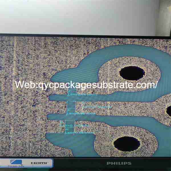
Signal Integrity: The design of ultra-small gap PCB structures is crucial for signal integrity. By delving into the PCB’s inter-layer and intra-layer wiring structures, one can better understand the signal transmission on the PCB, optimizing the design to reduce signal distortion and delay.
EMI (Electromagnetic Interference) and RFI (Radio Frequency Interference) Control: The structure of the PCB directly influences its electromagnetic and radiofrequency performance. A detailed study of ultra-small gap PCB structures can help identify and address potential electromagnetic compatibility issues, ensuring stable operation in high-speed communication environments.
Material Selection and Layer Design: Ultra-small gap PCBs often require the use of advanced materials to meet the demands of high frequencies and fast transmission. A deep understanding of PCB structures can assist in selecting appropriate materials and optimizing layer design to enhance performance.
Innovations in Manufacturing Processes: Studying the structure of ultra-small gap PCBs contributes to the discovery of new manufacturing processes. For example, adopting improved High-Density Interconnect (HDI) manufacturing techniques and emerging semi-additive methods may enhance manufacturing efficiency, reduce costs, and potentially offer higher performance.
Heat Dissipation and Thermal Management: The dense layout of high-speed electronic devices in ultra-small gap PCBs may pose challenges in heat dissipation and thermal management. In-depth knowledge of PCB structures can help optimize heat dissipation designs, ensuring stable performance under high loads.
Reliability and Lifespan: Structural improvements are closely related to the reliability and lifespan of the PCB. Understanding the fatigue characteristics of materials and electrical performance can optimize PCB design, prolonging the device’s operational lifespan.
In conclusion, a thorough study of the structure of ultra-small gap high-speed PCBs can offer crucial insights for the design and manufacturing of electronic devices, driving technological advancements and delivering exceptional performance.
What are the FAQs Surrounding Ultra-Small Gap High-Speed PCBs?
What is an ultra-small gap high-speed PCB?
An ultra-small gap high-speed PCB is specifically crafted for high-frequency applications, often operating in the gigahertz (GHz) range. The term “ultra-small gap” denotes the closely positioned traces and components on the board, a critical feature aimed at reducing signal interference and preserving signal integrity.
Why are ultra-small gaps necessary for high-speed PCBs?
Ultra-small gaps help control impedance and reduce signal reflections, crosstalk, and other high-frequency signal integrity issues. This is crucial for maintaining the quality of signals in high-speed electronic devices.
What challenges are associated with ultra-small gap high-speed PCB design?
Challenges include managing electromagnetic interference (EMI), maintaining controlled impedance, minimizing signal skew, and dealing with parasitic capacitance and inductance. Designers need to carefully consider materials, trace geometries, and the overall layout to address these challenges.
Which materials are suitable for ultra-small gap high-speed PCBs?
High-frequency laminates with low dielectric constant (Dk) and low dissipation factor (Df) are preferred. Materials like PTFE (Teflon) or specialty high-frequency prepregs are commonly used for their excellent electrical properties.
How does trace width and spacing affect signal integrity?
Trace width and spacing are critical parameters that affect impedance. Maintaining consistent trace dimensions helps control impedance, reduce crosstalk, and minimize signal distortion, ensuring reliable high-speed signal transmission.
Do I need to consider controlled impedance in all signal traces?
Yes, controlled impedance is crucial for high-speed signal integrity. While it may be more critical for certain signals like differential pairs, it is generally recommended to maintain controlled impedance across all high-speed signal traces.
What are the misconceptions about ultra-small gap high-speed PCBs?
One common misconception is that smaller gaps always lead to better performance. While minimizing gaps is essential, it’s equally important to strike a balance and consider other factors such as manufacturing tolerances and material properties.
How can simulation tools help in designing ultra-small gap high-speed PCBs?
Simulation tools can predict and analyze the behavior of high-speed signals on PCBs, helping designers identify and address potential issues before fabrication. This includes simulations for signal integrity, EMI, and power distribution.
Are there specific design guidelines for ultra-small gap high-speed PCBs?
Yes, there are design guidelines that cover aspects such as controlled impedance, signal routing, ground plane design, and thermal management. Following these guidelines is essential for achieving optimal performance in high-speed applications.
What are the manufacturing challenges associated with ultra-small gap high-speed PCBs?
Manufacturing ultra-small gap high-speed PCBs presents challenges such as stringent tolerances, meticulous material selection, and the need for sophisticated fabrication techniques. Seamless collaboration between designers and manufacturers is essential to accurately translate design intent into the final product, addressing these challenges effectively.
How Will Ultra-Small Gap High-Speed PCBs Shape the Future?
Ultra-small gap high-speed PCBs represent a significant technological innovation in the field of electronic design, exerting profound influence on the future development of electronics. Here are some key points on how this technology trend acts as a catalyst for innovation in electronics:
Higher Performance: Ultra-small gap high-speed PCBs allow for shorter signal transmission paths and lower signal latency, enabling electronic devices to achieve higher performance. This is essential for applications that entail the processing of extensive data volumes or demand swift responses, including high-performance computing, artificial intelligence, and communication systems.
Increased Integration: As the gaps within PCBs diminish, there arises an opportunity to densely arrange electronic components on the board. This results in increased integration, enabling devices to encompass a greater number of features and electronic elements within the same physical space. This, in turn, fuels the trend toward smaller and lighter devices.
Reduced Power Consumption:The reduction of signal paths and the minimization of electrical capacitance typically result in lower power consumption, a critical consideration for battery-powered mobile devices, Internet of Things (IoT) devices, and applications emphasizing energy efficiency. The incorporation of ultra-small gap high-speed PCBs significantly contributes to the progress in developing more energy-efficient electronic systems.
Enhanced Communication Reliability: For communication devices, the stability and reliability of signal transmission are crucial. Ultra-small gap high-speed PCBs contribute to minimizing signal distortion and interference, thereby enhancing the stability and overall performance of communication systems.
Advanced Application Areas: The advancement of this technology is poised to catalyze innovation in cutting-edge sectors like autonomous vehicles, medical devices, virtual reality, and beyond. These domains necessitate electronic devices that are not only high-performing but also reliable, and the integration of ultra-small gap high-speed PCBs plays a crucial role in fulfilling these demanding requirements.
In summary, the emergence of ultra-small gap high-speed PCBs signifies a major technological leap in electronic design. By providing higher performance, more compact designs, lower power consumption, and reliable communication, this technology trend will propel the development of electronic devices, paving the way for broader innovation in the future.