
What is Ultra-Small Pitch Substrates?
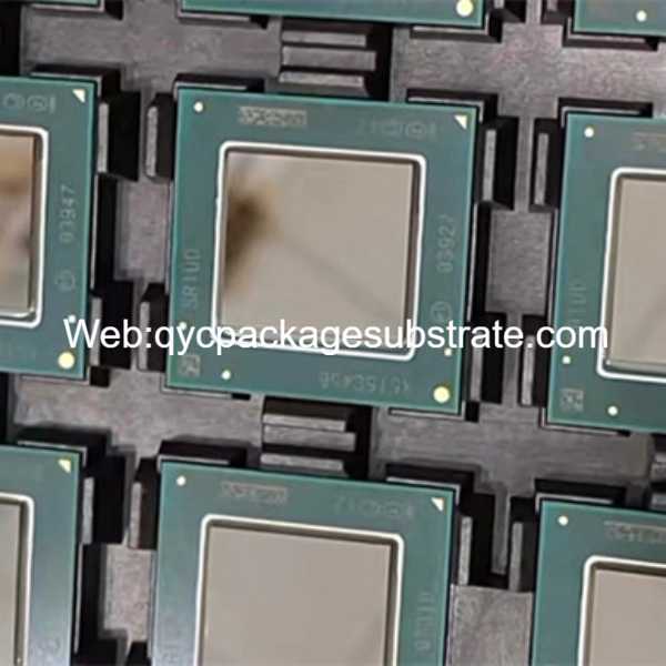
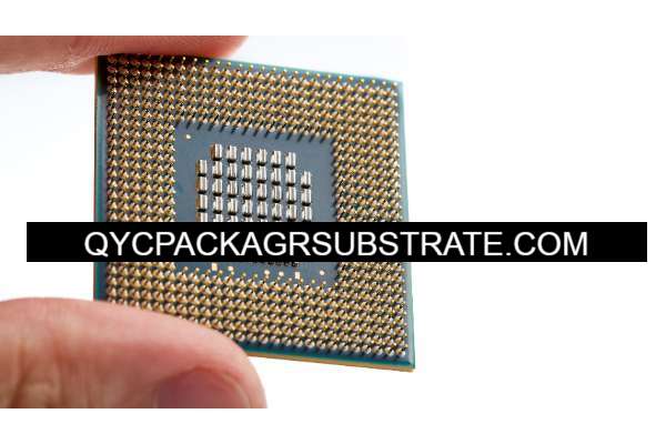
Ultra-small pitch substrateand package substrate manufacturer. We use advanced Msap and Sap technology, High multilayer interconnection substrates from 4 to 20 layers.
As of my last knowledge update in January 2022, the term “Ultra-Small Pitch Substrates” primarily refers to the substrate technology used in the construction of electronic devices, especially in the context of printed circuit boards (PCBs). The term signifies the reduced pitch or spacing between individual components or features on the substrate. The pitch is the distance between the center of one element to the center of the adjacent, similar element.
Here are some key points that may help unravel the intricacies of Ultra-Small Pitch Substrates:
Miniaturization: Ultra-small pitch substrates are designed to accommodate smaller and more closely spaced components on a PCB. This enables the downsizing of electronic devices, a critical factor in creating gadgets that are more compact and lightweight.
High-Density Interconnects:The decreased pitch in ultra-small substrates facilitates a high-density interconnection, permitting a greater number of components within the limited surface area of a PCB. This is especially critical in compact electronic devices like mobile gadgets and wearables, where space is at a premium.
Advanced Manufacturing Techniques: To achieve ultra-small pitches, sophisticated manufacturing techniques are essential. These include precision etching, laser drilling, and fine-pitch soldering. These processes demand an elevated level of precision and control to uphold the reliability and performance of electronic components.
Signal Integrity and Crosstalk Considerations:As components are positioned in closer proximity, ensuring the integrity of signals becomes a vital consideration.The proximity of traces and components can lead to signal crosstalk and interference. Engineers working with ultra-small pitch substrates must carefully design and analyze the layout to mitigate these issues.
Materials Innovation: The materials used in ultra-small pitch substrates play a crucial role in ensuring the reliability and performance of the PCB. Advanced materials with specific electrical and thermal properties are often employed to meet the demanding requirements of modern electronic devices.
Applications: Ultra-small pitch substrates find extensive applications in electronic devices like smartphones, tablets, wearables, and compact consumer electronics. Their utilization also extends to critical sectors such as high-performance computing, automotive electronics, and medical devices, where the emphasis on size, weight, and reliability is paramount. This technology’s broad adoption underscores its versatility across diverse industries and highlights its pivotal role in advancing miniaturization and enhancing the performance of various electronic systems.
Challenges: Ultra-small pitch substrates, despite their various benefits, pose challenges related to manufacturing intricacies, cost considerations, and potential reliability issues.Ensuring the robustness of the manufacturing process and addressing potential challenges is crucial for the widespread adoption of this technology.
It’s important to note that technology evolves rapidly, and advancements in ultra-small pitch substrates may have occurred since my last update. Engineers and researchers are continually pushing the boundaries of what is possible in PCB design to meet the demands of increasingly sophisticated and compact electronic devices.
How Do Ultra-Small Pitch Substrates Work?
Ultra-small pitch substrates refer to a specialized type of substrate technology utilized in the construction of electronic devices, particularly in printed circuit boards (PCBs). The term “pitch” denotes the spacing or distance between individual components on the substrate. Ultra-small pitch substrates are characterized by a significantly reduced pitch, enabling tighter integration of electronic components. Here’s an exploration of their core functionality and their impact on the performance, density, and miniaturization of electronic components:
Reduced Spacing: The primary characteristic of ultra-small pitch substrates is the diminished distance between individual elements on the PCB. This reduction in pitch allows electronic components to be placed closer together, facilitating higher component density on the same surface area.
Enhanced Miniaturization: By enabling components to be packed more densely, ultra-small pitch substrates contribute to the miniaturization of electronic devices. This is particularly crucial in industries where space constraints are a major consideration, such as consumer electronics and portable devices.
High-Density Interconnects: The reduced pitch supports high-density interconnects, meaning that a larger number of components can be interconnected on the PCB. This is essential for advanced electronic systems where numerous components must work seamlessly together, as seen in modern smartphones, tablets, and other complex electronic devices.
Improved Signal Integrity: While the compact arrangement of components poses challenges for signal integrity, ultra-small pitch substrates often incorporate advanced design techniques and materials to mitigate issues such as crosstalk and signal interference. This ensures that electronic signals maintain their integrity, contributing to the overall performance of the device.
Advanced Manufacturing Techniques: The manufacturing of ultra-small pitch substrates involves precise and advanced techniques such as precision etching, laser drilling, and fine-pitch soldering. These techniques are essential to achieve the required level of precision for the close arrangement of components.
Materials Innovation: The choice of materials for ultra-small pitch substrates is critical. Advanced materials with specific electrical, thermal, and mechanical properties are often employed to meet the demanding requirements of modern electronic devices, ensuring reliability and longevity.
Applications Across Industries: Ultra-small pitch substrates have diverse applications across various industries, including consumer electronics, high-performance computing, automotive electronics, and medical devices. Their adaptability makes them a key enabler in the development of innovative and compact electronic systems.
Size, Weight, and Reliability Considerations: In industries where size, weight, and reliability are critical factors, such as automotive and medical applications, ultra-small pitch substrates play a pivotal role. Their contribution to reducing the footprint of electronic components positively impacts the overall design and functionality of devices.
In summary, ultra-small pitch substrates work by enabling the close arrangement of electronic components, contributing to increased density, enhanced miniaturization, and improved overall performance in a wide range of electronic devices and applications.
Exploring the Versatility of Package Substrates
In the expansive domain of package substrates, ultra-small pitch substrates distinguish themselves with unique characteristics that contribute to their versatility across a spectrum of applications. These substrates, characterized by their reduced pitch or spacing between components, serve as a driving force in printed circuit board (PCB) innovation. Let’s delve into how ultra-small pitch substrates stand out and the diverse array of applications they cater to, spanning from consumer electronics to industrial use cases.
Consumer Electronics: Ultra-small pitch substrates play a pivotal role in the miniaturization of consumer electronics. Their ability to tightly pack components facilitates the creation of sleek and compact designs in devices like smartphones, tablets, and wearables, contributing to enhanced portability and user experience.
High-Performance Computing: In the realm of high-performance computing, where efficiency and power management are critical, ultra-small pitch substrates enable the integration of densely packed components. This feature is instrumental in applications such as data centers, supercomputers, and high-speed computing systems, fostering optimal performance.
Automotive Electronics: The automotive industry benefits from the versatility of ultra-small pitch substrates in electronic control units (ECUs), sensors, and infotainment systems. Their compact design addresses space constraints within vehicles while enhancing the reliability and performance of automotive electronics.
Medical Devices: Ultra-small pitch substrates find applications in the medical field, contributing to the development of advanced and compact medical devices. From implantable medical devices to diagnostic equipment, these substrates support the precision and reliability demanded by the medical industry.
Industrial Applications: In industrial settings, ultra-small pitch substrates are employed for control systems, monitoring devices, and automation equipment. Their capacity to withstand harsh environmental conditions, coupled with high-density interconnects, makes them well-suited for various industrial electronic applications.
Internet of Things (IoT): As the Internet of Things (IoT) ecosystem expands, ultra-small pitch substrates are instrumental in designing small, interconnected devices. They enable the development of IoT sensors and devices with reduced form factors, contributing to the proliferation of IoT applications across industries.
Aerospace and Defense: Ultra-small pitch substrates play a critical role in aerospace and defense applications, where both size and reliability are paramount. Used in avionics, radar systems, and communication equipment, these substrates contribute to weight reduction and efficient space utilization in aerospace electronics.
Wearable Technology: Wearables, including smartwatches and fitness trackers, benefit from ultra-small pitch substrates due to their support for component miniaturization. These substrates facilitate the creation of lightweight and compact wearables without compromising on performance.
Telecommunications: In the telecommunications industry, ultra-small pitch substrates are integral to the development of high-speed communication equipment, routers, and networking devices. Their high-density interconnects enhance the efficiency of data transmission within telecommunications infrastructure.
In summary, the versatility of ultra-small pitch substrates arises from their unique ability to support miniaturization, high-density interconnects, and advanced manufacturing techniques. These substrates serve as a driving force in PCB innovation, influencing the design and functionality of electronic devices across diverse industries.
How Does Ultra-Small Pitch Compare to Traditional PCBs?
A comparative analysis between ultra-small pitch substrates and traditional PCBs reveals notable differences in design, manufacturing processes, and performance metrics. Exploring these distinctions helps illustrate how the adoption of ultra-small pitch substrates can revolutionize PCB design and manufacturing.
Design:
Component Density: The most apparent difference lies in component density. Ultra-small pitch substrates allow for significantly higher component density due to the reduced spacing between elements. Traditional PCBs, with larger pitch values, are limited in the number of components that can be accommodated within a given area.
Miniaturization: Ultra-small pitch substrates excel in facilitating miniaturization. They enable the creation of smaller, more compact electronic devices compared to traditional PCBs, which may be bulkier due to the larger pitch and component spacing.
Manufacturing Processes:
Precision Techniques: Manufacturing ultra-small pitch substrates involves precision techniques such as fine-pitch soldering, laser drilling, and advanced etching processes. These techniques demand a higher level of precision compared to the manufacturing processes used for traditional PCBs.
Advanced Materials: Ultra-small pitch substrates often utilize advanced materials with specific electrical and thermal properties to meet the demands of miniaturized and high-performance electronics. Traditional PCBs may not require the same level of material sophistication.
Performance Metrics:
Signal Integrity: Ultra-small pitch substrates pose challenges to signal integrity due to the proximity of traces and components. However, advancements in design and materials are implemented to mitigate signal integrity issues. Traditional PCBs, with larger pitch values, may experience fewer signal integrity challenges.
Power Efficiency: The integration of densely packed components in ultra-small pitch substrates can enhance power efficiency, making them suitable for applications where energy consumption is critical. Traditional PCBs may not achieve the same level of power efficiency due to larger component spacing.
Applications:
Versatility: Ultra-small pitch substrates are highly versatile and find applications in consumer electronics, high-performance computing, automotive electronics, and medical devices. Traditional PCBs are still widely used across various applications but may be less suitable for miniaturized and high-density electronic designs.
Specific Use Cases: Traditional PCBs are often employed in applications where component density and miniaturization are not critical factors. These may include less space-constrained industrial applications, certain telecommunications equipment, and simpler electronic devices.
Complexity and Cost:
Manufacturing Complexity: Ultra-small pitch substrates, with their advanced manufacturing processes and materials, can be more complex to manufacture than traditional PCBs. This complexity can impact manufacturing costs and require specialized equipment and expertise.
Cost Considerations: While traditional PCBs are generally less complex to manufacture, resulting in lower production costs compared to ultra-small pitch substrates, the overall cost-effectiveness hinges on the specific requirements and constraints of the given application.
In conclusion, the integration of ultra-small pitch substrates signifies a revolutionary transformation in both PCB design and manufacturing. This shift is chiefly motivated by the pursuit of achieving miniaturization, elevating component density, and enhancing overall performance metrics.While traditional PCBs continue to serve various applications effectively, ultra-small pitch substrates offer a transformative approach for industries seeking compact, high-performance electronic solutions.
What Makes Up the Structure of Ultra-Small Pitch Substrates?
The structure of ultra-small pitch substrates is intricately designed to optimize compactness and performance. Several structural marvels define these substrates, each contributing to their unique capabilities. Let’s delve into the key components and manufacturing technologies that drive the innovation behind the structure of ultra-small pitch substrates:
Base Material:
High-Performance Substrate Materials: Ultra-small pitch substrates are often constructed using high-performance materials with specific electrical, thermal, and mechanical properties. These materials provide the necessary stability and performance for the compact and densely packed electronic components.
Layered Design:
Multilayer Configuration: Ultra-small pitch substrates typically feature a multilayered structure, allowing for the integration of complex circuits. The layered design supports high-density interconnects and facilitates the routing of signals between various components.
Conductor Traces:
Fine-Line Traces: The conductor traces on ultra-small pitch substrates are characterized by fine-line patterns. These fine-line traces enable the close arrangement of components and contribute to the high-density interconnectivity, a crucial factor in achieving miniaturization.
Dielectric Layers:
Thin Dielectric Layers: Dielectric layers provide insulation between conductor traces. In ultra-small pitch substrates, these layers are often engineered to be thin yet effective, minimizing the distance between conductive elements and supporting the reduction of overall substrate thickness.
Via Structures:
Microvias and Through-Holes: Advanced via structures, including microvias and through-holes, play a pivotal role in connecting different layers of the substrate. Microvias, in particular, enable the creation of compact interconnections, contributing to the substrate’s high-density design.
Surface Finish:
Advanced Surface Finishes: The surface finish of ultra-small pitch substrates is carefully chosen to enhance solderability and ensure the reliability of solder joints. Advanced surface finishes contribute to the substrates’ overall performance and longevity.
Advanced Manufacturing Techniques:
Precision Etching: Precision etching processes are employed to define intricate patterns for conductor traces on the substrate. This precision is crucial for achieving the fine-line features required for ultra-small pitch substrates.
Laser Drilling: Laser drilling is utilized to create microvias, enabling precise connections between different layers of the substrate. This technology supports the high-density interconnects necessary for compact electronic designs.
Fine-Pitch Soldering: Fine-pitch soldering techniques are applied during assembly to ensure the reliable connection of components with minimal spacing. This is essential for maintaining the structural integrity and functionality of the substrate.
Quality Control Measures:
High-Quality Standards: Due to the intricate nature of ultra-small pitch substrates, rigorous quality control measures are implemented throughout the manufacturing process. These measures help ensure the reliability and performance of the final product.
In summary, the structure of ultra-small pitch substrates is characterized by high-performance materials, a multilayered design, fine-line traces, advanced via structures, carefully chosen surface finishes, and the application of precise manufacturing technologies. These structural marvels collectively contribute to the unique capabilities of ultra-small pitch substrates, driving innovation in PCB design and manufacturing for compact and high-performance electronic devices.
What Are the Key Production Technologies for Ultra-Small Pitch Substrates?
The production of ultra-small pitch substrates relies on several key manufacturing technologies that enable the fabrication of these advanced components. These technologies contribute to the intricate design, high-density interconnects, and miniaturization required for ultra-small pitch substrates. Here are some of the key production technologies driving innovation in the fabrication of ultra-small pitch substrates:
High-Density Interconnect (HDI) Fabrication:
Microvia Formation: HDI fabrication involves the creation of microvias, which are small-diameter holes that connect different layers of the substrate. Microvias play a crucial role in achieving high-density interconnectivity.
Sequential Build-Up (SBU): SBU is a process where additional layers of copper and dielectric material are sequentially added to the substrate. This allows for the creation of complex multilayer structures with fine features.
Laser Drilling:
Precision Drilling of Microvias: Laser drilling is a precise technique used to create microvias with diameters in the micrometer range. This technology ensures accuracy in forming small holes for interconnection between substrate layers.
Fine-Pitch Soldering:
Solder Mask Application: Fine-pitch soldering involves the application of solder mask to define the areas where solder connections will be made. This process requires high precision to accommodate the reduced pitch between components.
Semi-Additive and Subtractive Processes:
Semi-Additive Manufacturing: In semi-additive processes, copper is selectively added to the substrate, allowing for more precise control over conductor trace patterns. This method is essential for achieving fine-line features in ultra-small pitch substrates.
Subtractive Etching: Subtractive processes involve selectively removing material from the substrate using chemical etching. This is a crucial step in defining the conductor traces and creating intricate patterns.
Advanced Surface Finishes:
Selective Surface Treatments: Advanced surface finishes, such as selective surface treatments, are applied to specific areas of the substrate to enhance solderability and ensure reliable connections. These treatments contribute to the overall quality and performance of the substrate.
High-Precision Imaging and Photolithography:
Photolithographic Techniques: High-precision imaging and photolithography are employed to transfer intricate patterns onto the substrate. This is a critical step in defining the layout of conductor traces and other features on ultra-small pitch substrates.
Materials Innovation:
High-Performance Substrate Materials: Innovations in substrate materials, including high-performance dielectrics and conductive materials, contribute to the reliability and performance of ultra-small pitch substrates. These materials are selected to meet the specific requirements of miniaturized and high-density electronic designs.
Quality Control and Inspection:
Advanced Inspection Techniques: Given the complexity of ultra-small pitch substrates, advanced inspection techniques, including automated optical inspection (AOI) and X-ray inspection, are employed to ensure the quality and reliability of the final product.
These production technologies collectively enable the fabrication of ultra-small pitch substrates, driving advancements in PCB manufacturing for applications that demand compact, high-density, and high-performance electronic components.
Can We Demystify Ultra-Small Pitch Substrates?
What distinguishes ultra-small pitch substrates from traditional PCBs?
Ultra-small pitch substrates differ from traditional PCBs in their reduced pitch, enabling tighter component spacing. This distinction allows for increased component density and miniaturization, making them ideal for applications where space is a premium.
Are ultra-small pitch substrates compatible with existing electronic components and technologies?
Generally, yes. While ultra-small pitch substrates are engineered for compatibility with a diverse array of electronic components, it’s essential to approach their integration with thorough consideration of each component’s unique requirements. Special attention should be paid to factors such as signal integrity and manufacturing processes to ensure seamless and reliable performance in electronic devices.
How do ultra-small pitch substrates impact signal integrity?
The close arrangement of components on ultra-small pitch substrates can pose challenges to signal integrity due to increased crosstalk and interference. However, advancements in design and materials are implemented to mitigate these issues, ensuring reliable signal performance.
What applications benefit most from ultra-small pitch substrates?
Ultra-small pitch substrates are utilized in sectors and devices where compactness, heightened component density, and improved performance hold significant importance. This encompasses a diverse range of industries, including consumer electronics, high-performance computing, automotive electronics, medical devices, and various other applications.
How do manufacturing costs for ultra-small pitch substrates compare to traditional PCBs?
Manufacturing ultra-small pitch substrates can be more complex and may involve advanced techniques, potentially leading to higher production costs compared to traditional PCBs. However, the overall cost-effectiveness depends on specific application requirements and benefits.
What role do materials play in the performance of ultra-small pitch substrates?
Materials are crucial in achieving the desired electrical, thermal, and mechanical properties. High-performance substrate materials contribute to the reliability and performance of ultra-small pitch substrates in demanding electronic applications.
Can existing PCB design tools accommodate the design intricacies of ultra-small pitch substrates?
PCB design tools are continually evolving to accommodate advanced technologies. Many modern design tools include features specifically tailored for high-density and miniaturized designs, allowing engineers to work with ultra-small pitch substrates effectively.
How do ultra-small pitch substrates contribute to advancements in IoT devices?
Ultra-small pitch substrates play a vital role in the development of compact and interconnected IoT devices. Their miniaturization capabilities support the design of sensors and devices with reduced form factors, crucial for the growth of the IoT ecosystem.
What performance benchmarks can be expected with ultra-small pitch substrates?
Performance benchmarks depend on specific application requirements. Ultra-small pitch substrates can contribute to improved power efficiency, reduced footprint, and enhanced reliability, making them suitable for applications demanding high performance in compact spaces.
Are Ultra-Small Pitch Substrates Paving the Way Forward?
Indeed, Ultra-Small Pitch Substrates are paving the way forward in the realm of electronic engineering. These substrates, characterized by their exceptionally small pitch or spacing between components, are at the forefront of technological advancements. Here are key reasons why Ultra-Small Pitch Substrates are playing a pivotal role in shaping the future:
Miniaturization Pioneer:
Ultra-Small Pitch Substrates are leading the charge in the miniaturization trend within the electronics industry. By allowing for tighter component packing and reduced distances between elements, they enable the creation of remarkably compact electronic devices.
High-Density Interconnects:
The hallmark of Ultra-Small Pitch Substrates lies in their high-density interconnects. These substrates facilitate intricate and closely packed wiring configurations, resulting in improved signal integrity and overall performance.
Advanced Manufacturing Techniques:
Leveraging cutting-edge manufacturing techniques such as High-Density Interconnect (HDI) and semi-additive methods, Ultra-Small Pitch Substrates achieve levels of precision that were once challenging to attain. These techniques contribute to the creation of intricate and densely packed substrate designs.
Versatility Across Industries:
Ultra-Small Pitch Substrates find applications across a spectrum of industries, from consumer electronics like smartphones and wearables to critical sectors such as medical devices and aerospace. Their versatility positions them as key components for a wide range of advanced electronic applications.
Integration with Emerging Technologies:
With emerging technologies such as 5G, Internet of Things (IoT), and artificial intelligence driving the next wave of innovation, Ultra-Small Pitch Substrates are poised to play a crucial role. Their ability to support high-performance and densely integrated circuits aligns with the demands of these transformative technologies.
Enhanced Thermal Management:
As devices become more compact and powerful, thermal management becomes a critical consideration. Ultra-Small Pitch Substrates often incorporate advanced thermal management solutions, ensuring optimal operating conditions for electronic components even in confined spaces.
Contributing to Sustainable Practices:
Ongoing research in materials and manufacturing processes aims to make Ultra-Small Pitch Substrates more sustainable. Efforts are being made to develop eco-friendly materials and practices, aligning with the industry’s commitment to environmental responsibility.
Driving Innovation in Packaging Technologies:
Ultra-Small Pitch Substrates are driving innovation in packaging technologies such as 3D integration and advanced system-in-package (SiP) designs. These advancements enable greater component density and enhanced performance in electronic devices.
In essence, Ultra-Small Pitch Substrates are not merely components in electronic devices; they represent a transformative force driving the future of electronic engineering. Their impact is seen in the relentless pursuit of miniaturization, high-density interconnects, and the integration of emerging technologies, making them indispensable in the dynamic landscape of modern electronics.