
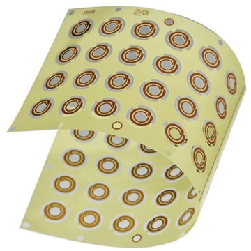
Ultrathin BT PCB manufacturing
We offer Ultrathin BT PCB, FR4 PCB. 1 layer or 2 layer PCB’s ultrathin thickness are 0.05mm(50um) , 0.07mm(70um). 0.1mm(100um). 0.12mm(120um). 0.15MM. the 4 layer and 6 layer PCB finished thickness are from 0.18mm(180um). 0.2mm(200um), 0.25mm to 0.6mm. We will produce the finished PCB boards thickness according to your requirements.
Ultrathin BT PCB manufacturing involves precision processes to create slim yet functional printed circuit boards tailored for Bluetooth technology applications. Utilizing specialized materials and advanced manufacturing techniques, Ultrathin BT PCBs are meticulously crafted to achieve compactness without compromising performance. From selecting thin laminates to precise etching and surface finishing, every step is optimized to ensure reliability and efficiency in wireless communication devices.
What is an Ultrathin BT PCB?
Ultrathin BT PCB manufacturing. we can produce the best samllest bump pitch with 100um, the best smallest trace are 9um. and the smallest gap are 9um. most of the design are 15um to 30um trace and spacing.
An Ultrathin BT PCB refers to an ultra-thin printed circuit board (PCB) designed for Bluetooth (BT) technology applications. Bluetooth is a wireless technology standard used for exchanging data over short distances between devices, such as smartphones, computers, and peripherals like keyboards and mice.
An ultrathin PCB is characterized by its extremely slim profile, often achieved by using specialized materials and manufacturing processes. These thin PCBs are particularly useful in applications where space is limited, such as in mobile devices, wearables, and other compact electronics.
The combination of Bluetooth technology with an ultrathin PCB allows for the creation of lightweight and compact devices that can wirelessly communicate with other Bluetooth-enabled devices, offering flexibility and convenience in various consumer and industrial applications.
What are the Ultrathin BT PCB Design Guidelines?
Here are some general design guidelines for Ultrathin BT PCBs:
- Select appropriate materials: Choose materials suitable for ultrathin PCBs, such as high-quality laminates and substrates that offer both flexibility and durability.
- Keep the PCB thin: Ensure the PCB thickness is minimized to meet the ultrathin requirement, typically by using thinner copper layers, thinner substrates, and reducing the number of layers if possible.
- Consider signal integrity: Pay close attention to signal integrity issues due to the thinness of the PCB. This may include impedance control, signal routing, and minimizing crosstalk and interference.
- Optimize component placement: Place components strategically to minimize the overall size of the PCB while ensuring efficient signal routing and thermal management.
- Use small form-factor components: Select components that are designed for compact PCB layouts, such as small surface-mount devices (SMDs) and fine-pitch integrated circuits (ICs).
- Implement proper grounding: Design a solid grounding scheme to minimize noise and ensure stable signal transmission, especially in high-frequency applications common in BT devices.
- Thermal management: Consider thermal dissipation requirements, especially if the device may generate heat during operation. Ensure proper ventilation and heat sinking strategies are implemented.
- Compliance with BT standards: Ensure that the PCB design complies with relevant Bluetooth standards and regulations to guarantee interoperability and reliability.
- Reliability testing: Perform rigorous testing and validation procedures to ensure the reliability and performance of the ultrathin BT PCB design under various operating conditions and environments.
By following these guidelines, designers can create ultrathin BT PCBs that meet the size, performance, and reliability requirements of modern Bluetooth-enabled devices.
Ultrathin BT PCB
What is the Ultrathin BT PCB Fabrication Process?
The fabrication process for ultrathin BT PCBs is similar to that of standard PCBs but with additional considerations for achieving the ultra-thin form factor. Here’s an overview of the fabrication process:
- Material Selection: Choose suitable materials that can meet the requirements for ultrathin PCBs. This may include thin laminates and substrates that offer flexibility and durability while still providing good electrical properties.
- Design Layout: Create the PCB layout using computer-aided design (CAD) software, taking into account the specific requirements for Bluetooth technology and the desired form factor. Ensure efficient use of space and optimized component placement.
- Photoresist Application: Apply a thin layer of photoresist onto the substrate material. This photoresist layer will be used to transfer the PCB pattern onto the substrate during the etching process.
- Exposure and Development: Use a photomask to expose the photoresist layer to UV light in the pattern of the desired circuit layout. Then, develop the exposed photoresist to remove the unexposed areas, leaving behind the patterned photoresist.
- Etching: Use chemical etching or another appropriate method to remove the exposed copper from the substrate, leaving only the copper traces of the desired circuit pattern.
- Surface Finishing: Apply surface finishes such as ENIG (Electroless Nickel Immersion Gold) or HASL (Hot Air Solder Leveling) to protect the copper traces and provide solderability for component attachment.
- Drilling: Use precision drilling equipment to create holes for component mounting and electrical connections. Ultrathin PCBs may require specialized drilling techniques to avoid damaging the delicate substrate.
- Component Attachment: Mount components onto the PCB using surface-mount technology (SMT) or through-hole technology (THT), depending on the design requirements and component types.
- Testing and Inspection: Conduct electrical testing and visual inspection to ensure the integrity and functionality of the ultrathin BT PCB. This may include continuity testing, impedance testing, and inspection for defects.
- Packaging and Shipping: Once the ultrathin BT PCBs pass inspection, they can be packaged and shipped to the assembly facility for integration into the final product.
Throughout the fabrication process, careful attention must be paid to maintaining the integrity of the ultrathin PCBs, as they are more susceptible to damage compared to standard PCBs due to their thinner profile. Specialized equipment and handling procedures may be necessary to ensure successful fabrication of ultrathin BT PCBs.
How do you manufacture an Ultrathin BT PCB?
Manufacturing an Ultrathin BT (Bluetooth) PCB involves several steps similar to the fabrication process of a standard PCB, with additional considerations for achieving the ultrathin profile. Here’s an overview of the typical fabrication process:
- Design: Create the PCB layout using computer-aided design (CAD) software, ensuring that the design meets the required specifications for the ultrathin BT application, including dimensions, component placement, and signal integrity considerations.
- Material selection: Choose materials suitable for ultrathin PCBs, such as thin laminates and substrates with appropriate dielectric properties. These materials should offer flexibility, heat resistance, and compatibility with the manufacturing process.
- Preparation of substrate: Prepare the substrate material by cutting it to the required dimensions and cleaning it to remove any contaminants that could affect the PCB manufacturing process.
- Copper deposition: Apply a thin layer of copper to one or both sides of the substrate using techniques like electroplating or chemical vapor deposition (CVD). The thickness of the copper layer should be optimized to minimize the overall thickness of the PCB.
- Photoresist application: Coat the copper-clad substrate with a layer of photoresist material. This photoresist layer will be used to transfer the PCB design onto the substrate during the imaging process.
- Exposure and development: Use a photomask to expose the photoresist layer to ultraviolet (UV) light, transferring the PCB design onto the photoresist. Then, develop the exposed photoresist to remove the unexposed areas, leaving behind the pattern of the PCB traces.
- Etching: Use chemical etching to remove the exposed copper areas not protected by the developed photoresist. This step defines the conductive traces on the PCB according to the design specifications.
- Photoresist stripping: Remove the remaining photoresist from the PCB surface, leaving behind the copper traces on the substrate.
- Surface finish: Apply surface finish to protect the exposed copper traces and ensure solderability. Common surface finish options include electroless nickel immersion gold (ENIG), immersion silver, and organic solderability preservatives (OSP).
- Drilling: Drill holes for through-hole components and vias, if required, using precision drilling equipment. The drill holes provide electrical connections between different layers of the PCB.
- Plating: Plate the drilled holes with a conductive material to create the vias, ensuring electrical continuity between layers.
- Solder mask application: Apply a solder mask over the entire surface of the PCB, leaving only the areas for soldering components exposed. The solder mask protects the PCB from environmental factors and prevents solder bridges during assembly.
- Silkscreen printing: Optionally, apply silkscreen printing to add component labels, reference designators, and other markings on the PCB surface for easier assembly and identification.
- Final inspection: Perform visual inspection and electrical testing to ensure the PCB meets quality standards and specifications.
- Routing and singulation: Cut the larger panel containing multiple PCBs into individual boards using a routing or singulation process.
- Packaging and shipping: Package the finished ultrathin BT PCBs securely for shipping to customers or assembly facilities.
Throughout the manufacturing process, precise control of parameters such as material thickness, copper deposition, and etching is crucial to achieve the desired ultrathin profile while maintaining the integrity and reliability of the PCB. Additionally, adherence to industry standards and quality assurance practices helps ensure the final product meets performance requirements for Bluetooth applications.
How much should an Ultrathin BT PCB cost?
The cost of an Ultrathin BT (Bluetooth) PCB can vary significantly depending on several factors, including:
- PCB size: Larger PCBs generally cost more due to the increased material and manufacturing complexity.
- Number of layers: Ultrathin BT PCBs can be single-sided, double-sided, or multilayered. Multilayered PCBs typically cost more due to the additional layers and complexity.
- Material: The choice of materials, such as substrate type and copper thickness, can impact the cost. High-quality materials optimized for ultrathin PCBs may be more expensive.
- Complexity of design: PCB designs with intricate layouts, fine traces, and dense component placement may require more advanced manufacturing techniques, increasing the cost.
- Surface finish: Different surface finishes, such as ENIG (electroless nickel immersion gold) or HASL (hot air solder leveling), have varying costs.
- Quantity: Economies of scale apply, meaning larger production quantities often result in lower per-unit costs.
- Lead time: Shorter lead times may incur additional costs for expedited manufacturing and shipping.
- Additional services: Services like impedance control, gold fingers, and special testing requirements can add to the overall cost.
As a rough estimate, the cost of an Ultrathin BT PCB can range from a few dollars for simple single-sided designs to several hundred dollars for complex multilayered PCBs with advanced features. For more accurate pricing, it’s recommended to consult with PCB manufacturers or use online PCB quoting tools, providing detailed specifications for your specific project.
What is Ultrathin BT PCB base material?
The base material for Ultrathin BT (Bluetooth) PCBs typically consists of thin laminates or substrates that provide the necessary electrical and mechanical properties while maintaining a slim profile. Some commonly used base materials for ultrathin PCBs include:
- Flexible substrates: Flexible materials like polyimide (PI) or polyester (PET) are often used for ultrathin PCBs due to their ability to bend and conform to irregular shapes. These substrates are lightweight and offer good heat resistance, making them suitable for applications where flexibility is required.
- Rigid-flex substrates: Rigid-flex PCBs combine both rigid and flexible substrates, offering the advantages of both types of materials. They are used in applications where a combination of flexibility and rigidity is needed, such as in foldable devices or wearables.
- Thin laminates: Specialized thin laminates with reduced thicknesses are used to create ultrathin PCBs while maintaining the necessary electrical insulation and mechanical strength. These laminates may include materials like thin FR-4 (glass-reinforced epoxy) or other high-performance substrates.
- Metal core substrates: Metal core PCBs utilize a metal core, such as aluminum or copper, as the base material instead of traditional rigid or flexible substrates. These substrates offer excellent thermal conductivity and can help dissipate heat efficiently, making them suitable for high-power applications.
- Specialized materials: Some ultrathin PCBs may require specialized materials tailored to specific performance requirements, such as high-frequency laminates for RF applications or high-temperature materials for harsh environments.
The choice of base material depends on factors such as the application requirements, desired flexibility, thermal considerations, and manufacturing capabilities. Designers must select a base material that balances these factors while meeting the performance and reliability requirements of the Ultrathin BT PCB.
Which company makes Ultrathin BT PCB?
Many companies offer manufacturing services for Ultrathin BT PCBs, including large PCB manufacturers, specialized firms focusing on flexible electronics, and custom PCB suppliers. Our company also provides production services for Ultrathin BT PCBs.
We have advanced manufacturing equipment and an experienced technical team capable of meeting the manufacturing needs of Ultrathin PCBs. Our manufacturing process is refined to ensure the production of high-quality, reliable products. Here are some key features of the Ultrathin BT PCB production services we offer:
- Professional design team: We have an experienced design team capable of designing layouts and structures that meet the requirements and specifications of Ultrathin BT PCBs.
- Advanced manufacturing equipment: Our manufacturing facility is equipped with state-of-the-art production equipment, including precision PCB manufacturing equipment and automated production lines, capable of meeting the manufacturing requirements of Ultrathin PCBs.
- Quality control and testing: We strictly adhere to quality control standards, conducting rigorous inspections and testing at every stage from raw material procurement to final product delivery to ensure consistent and reliable product quality.
- Customization services: We offer customization services to meet the specific requirements of our customers, including special material selection and process requirements.
- Timely delivery: We have flexible production scheduling to ensure on-time delivery of customer orders, meeting their production needs.
Through our company’s production capabilities and professional expertise, we can provide high-quality, customized production services for Ultrathin BT PCBs, meeting the requirements of various application scenarios.
What are the 7 qualities of good customer service?
Good customer service is characterized by several key qualities that contribute to positive interactions and relationships with customers. Here are seven qualities of good customer service:
- Responsiveness: Good customer service involves promptly addressing customer inquiries, concerns, and requests. Responding to customers in a timely manner demonstrates attentiveness and a commitment to meeting their needs.
- Empathy: Empathy involves understanding and showing compassion for the customer’s perspective, emotions, and situation. Listening actively, acknowledging their feelings, and demonstrating understanding can help build rapport and trust.
- Clear communication: Effective communication is essential for conveying information clearly and accurately. Good customer service representatives communicate in a friendly, professional manner, using language that is easy to understand and free of jargon.
- Problem-solving skills: Good customer service involves efficiently resolving issues and finding solutions to customer problems. Customer service representatives should be proactive, resourceful, and empowered to address customer concerns effectively.
- Product knowledge: Knowledgeable customer service representatives can provide accurate information about products or services, answer questions, and offer helpful recommendations. They stay informed about product features, benefits, and policies to assist customers effectively.
- Professionalism: Professionalism entails maintaining a positive attitude, remaining calm under pressure, and conducting oneself with integrity and respect. Good customer service representatives demonstrate professionalism in their interactions with customers, colleagues, and stakeholders.
- Follow-up: Following up with customers after resolving an issue or completing a transaction demonstrates attentiveness and a commitment to customer satisfaction. Good customer service includes checking in with customers to ensure their needs have been met and addressing any further concerns.
By embodying these qualities, businesses can cultivate positive customer experiences, foster loyalty, and build lasting relationships with their customers.
FAQs (Frequently Asked Questions)
What are the advantages of Ultrathin BT PCBs?
Ultrathin BT PCBs offer excellent thermal performance, high electrical insulation, and reliability, making them suitable for compact electronic devices and applications where space is limited.
Can Ultrathin BT PCBs withstand high temperatures?
Yes, Ultrathin BT PCBs are designed to withstand elevated temperatures, making them suitable for applications requiring thermal stability.
What is the maximum thickness of an Ultrathin BT PCB?
Ultrathin BT PCBs typically have a thickness ranging from 0.2mm to 0.8mm, although custom thicknesses can be accommodated based on specific requirements.
Are Ultrathin BT PCBs suitable for flexible applications?
While Ultrathin BT PCBs are not inherently flexible, they offer flexibility in terms of design and can be adapted for applications requiring a slim profile and high performance.
What surface finishes are available for Ultrathin BT PCBs?
Common surface finishes for Ultrathin BT PCBs include ENIG (Electroless Nickel Immersion Gold), HASL (Hot Air Solder Leveling), and immersion silver, among others, each offering different properties and benefits.