
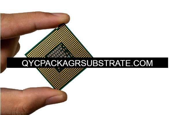
Ultrathin GPU Package Substrate Manufacturer
Ultrathin GPU Package Substrate Manufacturer,Ultrathin GPU Package Substrates are specialized components designed for high-performance graphics processing units (GPUs). These substrates feature an exceptionally thin profile, optimizing space within compact electronic devices while maintaining robust structural integrity. Engineered with advanced materials like thin-film polymers or reinforced ceramics, they offer superior thermal management and electrical insulation properties crucial for GPU operation. Ultrathin GPU Package Substrates support the demanding requirements of modern graphics-intensive applications, such as gaming consoles, graphic design workstations, and artificial intelligence systems. Their innovative design enhances heat dissipation efficiency and minimizes signal loss, ensuring reliable performance and longevity in high-performance computing environments.
What is an Ultrathin GPU Package Substrate?
An Ultrathin GPU Package Substrate refers to a specialized substrate designed for graphics processing units (GPUs) that emphasizes a thin profile while maintaining high performance and reliability. These substrates are crucial in modern GPUs where space constraints and thermal management are critical factors.
Typically, Ultrathin GPU Package Substrates utilize advanced materials and manufacturing processes to achieve their slim profile without compromising on electrical performance or thermal dissipation capabilities. This includes considerations for materials like high-density interconnect (HDI) substrates, which offer improved signal integrity and thermal management.
Manufacturers often employ technologies such as embedded passive components and advanced thin-film processing to optimize these substrates further. This allows for denser packaging of components while reducing overall form factor, essential for integrating GPUs into compact devices like laptops, tablets, and mobile devices.
In summary, Ultrathin GPU Package Substrates are tailored to meet the demanding requirements of high-performance graphics processing in a compact form factor, ensuring efficiency, reliability, and optimal thermal management.
Ultrathin GPU Package Substrate Manufacturer
What are the Ultrathin GPU Package Substrate Design Guidelines?
Design guidelines for Ultrathin GPU Package Substrates focus on several key aspects to ensure optimal performance, reliability, and manufacturability. Here are some essential guidelines:
- Material Selection: Choose high-performance materials with excellent thermal conductivity and electrical properties, such as high-density interconnect (HDI) substrates or advanced laminates with low dielectric loss.
- Thin Profile: Ensure the substrate is designed to be ultrathin, typically less than 100 micrometers thick, to meet space constraints and improve thermal dissipation.
- Heat Dissipation:Optimize thermal management by integrating thermal vias, heatsinks, or thermal pads to efficiently dissipate heat generated by the GPU.
- Signal Integrity: Implement controlled impedance traces and minimize signal loss to maintain high-speed signal integrity, critical for GPU performance.
- Power Delivery: Design power distribution networks (PDNs) with low impedance paths and adequate decoupling capacitors to ensure stable power delivery to the GPU and associated components.
- Manufacturability: Consider manufacturability aspects such as panel size, layer count, and compatibility with assembly processes like flip-chip bonding or wire bonding.
- Reliability: Design for reliability by accounting for factors such as mechanical stress during assembly, thermal cycling, and compatibility with environmental conditions.
- EMI/EMC Considerations: Incorporate design techniques to mitigate electromagnetic interference (EMI) and ensure compliance with electromagnetic compatibility (EMC) standards.
- Cost Optimization: Balance performance requirements with cost considerations by optimizing material usage, layer stack design, and manufacturing processes.
- Testing and Validation: Include provisions for testing and validation of substrate prototypes to ensure they meet electrical, thermal, and mechanical specifications before mass production.
By adhering to these design guidelines, engineers can develop Ultrathin GPU Package Substrates that meet the stringent performance requirements of modern graphics processing units while maintaining reliability and manufacturability.
What is the Ultrathin GPU Package Substrate Fabrication Process?
The fabrication process for Ultrathin GPU Package Substrates involves several specialized steps to achieve the desired thin profile, high performance, and reliability. Here are the key stages typically involved:
- Material Selection: Choose high-performance substrates such as advanced laminates or high-density interconnect (HDI) materials with specific thermal, electrical, and mechanical properties suitable for GPU applications.
- Layer Stack Design: Design the substrate’s layer stack considering signal integrity, power distribution, and thermal management requirements. This includes determining the number of layers and the arrangement of conductive and insulating layers.
- Circuit Patterning: Use advanced lithography techniques to pattern the conductive traces and vias on the substrate layers. This process ensures precise routing of electrical signals and power distribution paths.
- Via Formation: Create vias (plated or filled) to establish electrical connections between different layers of the substrate. Thermal vias are also incorporated to facilitate heat dissipation from the GPU.
- Embedding Components: Utilize embedded passive components and thin-film technologies to integrate capacitors, resistors, and other components directly into the substrate layers. This enhances electrical performance while minimizing space and improving reliability.
- Surface Finish: Apply appropriate surface finishes to the substrate, such as immersion gold or tin, to ensure reliable electrical contacts and solderability during assembly.
- Thinning Process: Implement specialized thinning techniques to reduce the substrate thickness to the required ultrathin level, typically less than 100 micrometers. This may involve mechanical grinding, chemical etching, or laser ablation under precise control to maintain uniformity and integrity.
- Lamination and Pressing: If using multilayer construction, laminate and press the substrate layers together under controlled temperature and pressure. This step ensures bonding and integrity of the entire substrate structure.
- Quality Control and Testing:Conduct rigorous quality control checks and testing throughout the fabrication process. This includes inspection for defects, dimensional accuracy, electrical continuity, and thermal performance to meet stringent GPU specifications.
- Final Assembly: Prepare the substrate for final assembly with the GPU and other components. This may involve applying thermal interface materials, attaching heat sinks or thermal pads, and ensuring proper alignment and connection with the GPU package.
- Packaging and Protection:Package the completed substrate to protect it from environmental factors and mechanical stress during handling, shipping, and installation.
By following these fabrication steps with precision and utilizing advanced materials and processes, manufacturers can produce Ultrathin GPU Package Substrates that meet the demanding requirements of modern graphics processing while ensuring high performance, reliability, and thermal efficiency.
How do you manufacture an Ultrathin GPU Package Substrate?
Manufacturing an Ultrathin GPU Package Substrate involves a series of specialized steps designed to achieve a thin profile while maintaining high performance and reliability. Here’s a detailed outline of the typical manufacturing process:
- Material Selection: Choose advanced materials such as high-density interconnect (HDI) substrates or specialized laminates with excellent thermal conductivity and electrical properties suitable for GPU applications.
- Design and Layout: Design the substrate layout considering signal integrity, power distribution, and thermal management requirements. Determine the layer stack configuration and the placement of vias, components, and traces.
- Circuit Patterning: Utilize advanced lithography and etching techniques to pattern conductive traces and vias on the substrate layers. This step ensures precise routing of electrical signals and power distribution paths.
- Embedding Components: Integrate passive components (capacitors, resistors) and thin-film technologies directly into the substrate layers to enhance electrical performance and minimize space.
- Thinning Process: Employ specialized thinning techniques such as mechanical grinding, chemical etching, or laser ablation to reduce the substrate thickness to less than 100 micrometers. Ensure uniformity and integrity throughout the thinning process.
- Surface Treatment: Apply surface finishes such as immersion gold or tin to ensure reliable electrical contacts and solderability during assembly.
- Lamination and Bonding: If using multilayer construction, laminate and bond the substrate layers together under controlled temperature and pressure. This step ensures proper bonding and integrity of the substrate structure.
- Quality Control: Conduct rigorous quality control inspections throughout the manufacturing process. Check for defects, dimensional accuracy, electrical continuity, and thermal performance to meet GPU specifications.
- Thermal Management Integration: Incorporate thermal management features such as thermal vias, heatsinks, or thermal pads to facilitate heat dissipation from the GPU.
- Assembly and Packaging: Prepare the substrate for final assembly with the GPU and other components. Apply necessary thermal interface materials, attach heatsinks or thermal pads, and ensure proper alignment and connection with the GPU package.
- Testing and Validation: Perform comprehensive testing and validation of the completed substrate to verify electrical performance, thermal efficiency, and reliability under operational conditions.
- Packaging and Protection: Package the finished substrate to protect it from environmental factors and mechanical stress during transportation, handling, and installation.
By following these manufacturing steps with precision and utilizing advanced materials and techniques, manufacturers can produce Ultrathin GPU Package Substrates that meet the demanding requirements of high-performance graphics processing in a compact form factor, ensuring efficiency, reliability, and optimal thermal management.
How much should an Ultrathin GPU Package Substrate cost?
The cost of an Ultrathin GPU Package Substrate can vary widely depending on several factors, including:
- Material Costs: The type and quality of materials used in the substrate, such as advanced laminates or high-density interconnect (HDI) substrates, significantly impact costs.
- Manufacturing Complexity:The complexity of the substrate design, including the number of layers, embedded components, and special features like thermal management solutions, affects manufacturing costs.
- Fabrication Techniques: Specialized thinning processes, advanced lithography, and embedding technologies add to production costs due to their precision and specialized equipment requirements.
- Quality and Reliability Requirements: Meeting stringent quality control standards and reliability testing increases manufacturing costs to ensure the substrate meets performance specifications.
- Volume and Scale: Economies of scale play a crucial role; larger production volumes typically reduce per-unit costs due to optimized manufacturing processes and bulk material purchasing.
- Market Demand: Supply and demand dynamics in the semiconductor and electronics industry can influence substrate costs, especially for specialized components like Ultrathin GPU Package Substrates.
While specific cost figures can vary based on these factors and market conditions, Ultrathin GPU Package Substrates are generally priced higher than standard substrates due to their specialized design, advanced materials, and precision manufacturing requirements. As a rough estimate, costs can range from several dollars to tens of dollars per substrate unit, depending on the above factors and the supplier’s pricing structure.
What is Ultrathin GPU Package Substrate base material?
The base materials used for Ultrathin GPU Package Substrates typically include advanced laminates or high-density interconnect (HDI) substrates. These materials are chosen for their superior thermal conductivity, excellent electrical properties, and the ability to maintain structural integrity while being thin.
- Advanced Laminates:These are engineered materials that combine layers of fiberglass reinforced with resin and copper foil. They offer good thermal management capabilities and are suitable for high-speed signal transmission.
- High-Density Interconnect (HDI) Substrates: HDI substrates feature very fine lines and spaces, allowing for compact circuit designs. They are often used in multilayer substrates where space is limited, and thermal dissipation is crucial.
- Specialized Composites: Some substrates may use specialized composites that enhance specific properties like thermal conductivity or reduce the dielectric constant, improving signal integrity.
These materials are selected based on their ability to meet the demanding requirements of GPUs, including thermal management, electrical performance, and mechanical stability, all while achieving the ultrathin profile necessary for compact device designs.
Which companies make Ultrathin GPU Package Substrates?
Currently, several companies specialize in manufacturing Ultrathin GPU Package Substrates, focusing on advanced technologies in the semiconductor and electronics manufacturing sectors. These companies utilize advanced materials and manufacturing processes to meet the demands of high-performance Graphics Processing Units (GPUs), including thermal management, electrical performance, and mechanical stability.
Some well-known manufacturers include:
- Micron Technology: Micron provides advanced packaging solutions for high-performance GPUs using its advanced semiconductor manufacturing processes and material technologies.
- Intel: Intel, with its deep technical expertise in processors, also supports various GPU products through advanced packaging technologies.
- Taiwan Semiconductor Manufacturing Company (TSMC): As a global leader in semiconductor manufacturing services, TSMC offers highly customized packaging solutions for multiple GPU manufacturers.
- United Microelectronics Corporation (UMC): UMC also has significant capabilities in advanced packaging technologies, providing customized support for GPU manufacturers.
- Samsung Electronics: Samsung offers high-performance packaging solutions for global GPU manufacturers using its advanced semiconductor materials and packaging technologies.
- BOE Technology: As a leading company in display technologies, BOE has also ventured into packaging technologies, supporting the production of various high-performance GPUs.
Our company is also capable of producing Ultrathin GPU Package Substrates. We possess advanced manufacturing equipment and a skilled technical team capable of customizing high-performance GPU packaging solutions according to customer requirements. Our production processes strictly adhere to industry standards and quality management systems to ensure that each substrate meets the technical specifications and quality standards of our customers. Moreover, we focus on technological innovation and continuous improvement to address rapidly changing market demands, providing reliable packaging solutions to our customers.
What are the 7 qualities of good customer service?
Good customer service is characterized by several key qualities that contribute to positive interactions and long-term customer satisfaction. Here are seven essential qualities:
- Responsiveness: Responding promptly to customer inquiries, concerns, or issues demonstrates attentiveness and shows that the customer’s time and needs are valued.
- Empathy: Showing empathy involves understanding and acknowledging the customer’s emotions, concerns, or frustrations. It involves putting oneself in the customer’s shoes to better address their needs.
- Patience: Patience is crucial, especially when dealing with challenging situations or customers who may be upset or unclear. Maintaining composure and taking the time to listen and assist without rushing can greatly improve the customer experience.
- Clear Communication: Effective communication involves being clear, concise, and courteous in all interactions. It includes actively listening to the customer, asking clarifying questions, and providing information in a way that is easy to understand.
- Knowledgeability: Having a good understanding of the products or services offered allows customer service representatives to provide accurate information and solutions. Knowledgeability instills confidence in customers and enhances their trust in the company.
- Professionalism: Maintaining a professional demeanor in all interactions, whether over the phone, email, or in-person, is essential. This includes being respectful, courteous, and maintaining confidentiality when handling customer information.
- Problem-solving Skills: Being able to effectively identify and resolve customer issues or complaints demonstrates proactive problem-solving skills. This may involve escalating issues when necessary and following up to ensure the customer’s needs are met.
These qualities collectively contribute to creating a positive customer service experience, fostering customer loyalty, and enhancing the overall reputation of the company.
FAQs
What is an Ultrathin GPU Package Substrate?
An Ultrathin GPU Package Substrate is a specialized type of substrate used in the packaging of Graphics Processing Units (GPUs). These substrates are characterized by their very thin profiles, typically less than 100 micrometers, and are designed to provide high performance, efficient thermal management, and reliable electrical connections in compact GPU designs.
Why are Ultrathin GPU Package Substrates important?
Ultrathin GPU Package Substrates are crucial because they enable the production of thinner and more compact GPUs, which are essential for modern electronics where space is limited. They also enhance thermal dissipation, support high-speed signal integrity, and ensure reliable power delivery, which are critical for the performance and longevity of GPUs.
What materials are used in Ultrathin GPU Package Substrates?
These substrates are typically made from advanced laminates or high-density interconnect (HDI) materials. These materials are chosen for their excellent thermal conductivity, electrical properties, and ability to maintain structural integrity despite being very thin.
How are Ultrathin GPU Package Substrates manufactured?
The manufacturing process involves several steps, including material selection, circuit patterning, via formation, embedding components, thinning processes, lamination, surface treatment, quality control, thermal management integration, assembly, and final packaging. Each step requires precision and advanced technologies to ensure the substrates meet the demanding requirements of high-performance GPUs.
What are the key design considerations for Ultrathin GPU Package Substrates?
Design considerations include selecting appropriate materials, optimizing thermal management, ensuring signal integrity, designing reliable power delivery networks, maintaining manufacturability, considering electromagnetic interference (EMI) and electromagnetic compatibility (EMC), balancing cost, and ensuring comprehensive testing and validation.
Which companies manufacture Ultrathin GPU Package Substrates?
Several leading companies specialize in the production of these substrates, including Micron Technology, Intel, Taiwan Semiconductor Manufacturing Company (TSMC), United Microelectronics Corporation (UMC), Samsung Electronics, and BOE Technology. Our company also produces Ultrathin GPU Package Substrates, offering advanced manufacturing capabilities and customized solutions.
How much do Ultrathin GPU Package Substrates cost?
The cost can vary widely depending on factors such as material quality, manufacturing complexity, volume, and market conditions. Generally, due to their specialized nature and advanced manufacturing processes, Ultrathin GPU Package Substrates are priced higher than standard substrates, with costs ranging from several dollars to tens of dollars per unit.
What are the applications of Ultrathin GPU Package Substrates?
These substrates are used in various high-performance computing applications, including gaming consoles, workstations, data centers, and professional graphics solutions. Their thin profile and efficient thermal management make them suitable for compact and high-performance GPU designs.
What are the benefits of using Ultrathin GPU Package Substrates?
Benefits include reduced overall package thickness, improved thermal dissipation, enhanced electrical performance, and the ability to support high-speed signal transmission. These advantages contribute to the development of more powerful and efficient GPUs in smaller form factors.