
Ultrathin High Speed Substrates Manufacturer
Ultrathin High Speed Substrates Manufacturer,Ultrathin High-Speed Substrates are advanced circuit board materials engineered for high-frequency applications requiring minimal thickness without compromising performance. These substrates are designed to handle rapid signal transmission and high-speed data processing while maintaining signal integrity and minimizing signal loss. Their ultrathin profile allows for compact and lightweight electronic devices, making them ideal for applications in telecommunications, high-speed computing, and consumer electronics. Typically made from advanced materials with low dielectric loss and high thermal conductivity, ultrathin high-speed substrates ensure efficient performance and reliability in demanding electronic environments, supporting the growing need for fast and efficient technology.
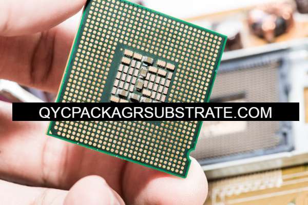
What is Ultrathin High Speed Substrates?
Ultrathin High-Speed Substrates are specialized printed circuit boards (PCBs) designed to meet the rigorous demands of high-speed electronic applications while maintaining an exceptionally thin profile. These substrates are crucial in modern electronics, where minimizing signal loss, reducing latency, and improving overall performance are essential.
The primary characteristic of ultrathin high-speed substrates is their reduced thickness, often significantly thinner than standard PCBs. This reduction in thickness contributes to several benefits, including lighter weight and more compact designs, which are particularly important in space-constrained applications such as mobile devices, wearables, and high-performance computing systems.
High-speed performance in these substrates is achieved through the use of advanced materials and design techniques. They often incorporate high-frequency laminate materials that minimize signal degradation and maintain integrity at high data rates. The substrates are engineered to support fast signal transitions and reduce electromagnetic interference (EMI), which is critical for maintaining signal fidelity in high-speed communication.
Design considerations for ultrathin high-speed substrates include precise layer stacking, controlled impedance traces, and optimal via placements to ensure signal integrity and thermal management. The manufacturing process also emphasizes high precision to maintain the thin profile while achieving the required electrical performance.
These substrates are used in a variety of applications, including high-frequency RF circuits, high-speed data communication systems, and advanced consumer electronics. Their ability to deliver high performance while adhering to strict size constraints makes them indispensable in the rapidly evolving field of electronics.
Ultrathin High Speed Substrates Manufacturer
What are the Design Guidelines for Ultrathin High Speed Substrates?
Designing ultrathin high-speed substrates involves several critical guidelines to ensure optimal performance and reliability. Here are the key considerations:
- Material Selection: Choose high-frequency laminate materials with low dielectric loss and stable electrical properties. Materials such as PTFE (polytetrafluoroethylene) or advanced ceramics are commonly used to minimize signal attenuation and maintain signal integrity at high speeds.
- Layer Stacking:Carefully plan the layer stack-up to manage impedance and reduce signal degradation. The arrangement of dielectric and conductive layers should be optimized for high-speed signal transmission, ensuring consistent impedance and minimizing cross-talk.
- Controlled Impedance: Design traces with controlled impedance to prevent signal reflection and loss. Use impedance calculators and simulation tools to ensure that trace widths and spacing match the required impedance values for high-speed signals.
- Via Design: Minimize the number and size of vias, as they can introduce signal loss and affect performance. When vias are necessary, use blind or buried vias to reduce their impact on signal integrity and thermal management.
- Thermal Management: Incorporate effective thermal management techniques to dissipate heat generated by high-speed components. This may include thermal vias, heat sinks, or copper pours to ensure reliable operation and prevent overheating.
- Signal Integrity: Implement techniques to preserve signal integrity, such as differential pair routing, proper shielding, and reducing trace lengths. Avoid sharp corners and sudden changes in trace width to minimize signal reflections and impedance discontinuities.
- Electromagnetic Interference (EMI): Design to minimize EMI by using shielding techniques, ground planes, and careful trace routing. Ensure that high-speed traces are well-isolated from sensitive areas and other high-current traces.
- Manufacturing Tolerances: Account for manufacturing tolerances in your design to ensure that the final product meets performance specifications. Work closely with the PCB manufacturer to understand their capabilities and limitations regarding ultrathin substrates.
- Simulation and Testing:Utilize simulation tools to model the electrical and thermal performance of the substrate before manufacturing. Conduct thorough testing to validate the design and identify potential issues that could impact high-speed performance.
By adhering to these guidelines, designers can create ultrathin high-speed substrates that meet the demanding requirements of modern electronics while ensuring reliability and performance.
What is the Fabrication Process for Ultrathin High Speed Substrates?
The fabrication process for ultrathin high-speed substrates involves several specialized steps to ensure high performance and precision. Here’s an overview of the key stages:
- Material Preparation: The process begins with selecting and preparing high-frequency laminate materials suited for ultrathin substrates. These materials are chosen for their low dielectric loss, stable electrical properties, and thin profiles. Common materials include PTFE (polytetrafluoroethylene) or advanced ceramics.
- Lamination: Thin layers of laminate material are stacked and laminated together using high-pressure and high-temperature presses. The lamination process bonds the layers into a cohesive substrate while maintaining their thin profile and desired electrical properties.
- Patterning: The next step involves patterning the substrate to define the circuit traces and pads. This is typically done using photolithography, where a photoresist layer is applied to the substrate, exposed to UV light through a mask, and then developed to reveal the pattern. The exposed areas are then etched away to create the desired circuit patterns.
- Etching:The etching process removes unwanted copper or other conductive material from the substrate to form the circuit traces. Techniques such as chemical etching or plasma etching are used to achieve precise and clean patterns.
- Drilling: Vias, which are small holes that connect different layers of the substrate, are drilled using high-precision lasers or mechanical drills. For ultrathin substrates, minimizing the number and size of vias is crucial to maintain signal integrity and performance.
- Plating: After drilling, the vias and circuit traces are plated with a thin layer of metal, typically copper, to enhance conductivity. This is done through electroplating or electroless plating processes.
- Insulation: Additional layers of dielectric material may be applied to insulate the circuits and prevent short circuits. These insulating layers are carefully chosen to ensure they do not affect the high-speed performance of the substrate.
- Testing and Inspection: The fabricated substrate undergoes rigorous testing and inspection to verify its performance and adherence to specifications. Tests may include electrical testing for signal integrity, thermal analysis, and visual inspection for defects.
- Cutting and Finishing: Finally, the substrate is cut to its final dimensions and undergoes finishing processes, such as edge plating or surface coating, to ensure it meets all design requirements and is ready for integration into electronic devices.
By carefully managing each step of the fabrication process, manufacturers can produce ultrathin high-speed substrates that meet the demanding requirements of modern electronics while ensuring high performance and reliability.
How Do You Manufacture Ultrathin High Speed Substrates?
Manufacturing ultrathin high-speed substrates involves a series of precise and specialized steps to achieve the required thin profile and high-performance characteristics. Here’s a detailed overview of the manufacturing process:
- Material Selection: Begin by choosing high-frequency laminate materials known for their low dielectric loss and high-speed performance. Materials such as PTFE (polytetrafluoroethylene), high-performance ceramics, or advanced epoxy resins are commonly used. The choice of material is crucial for ensuring the substrate can handle high-speed signal transmission with minimal attenuation.
- Substrate Preparation: The laminate material is prepared and cut into thin sheets that match the desired thickness for the substrate. These sheets are then cleaned and prepped for lamination to remove any contaminants that could affect adhesion and performance.
- Lamination: Stack the prepared laminate sheets to form the multilayer substrate. The layers are aligned precisely and laminated under high pressure and temperature using a press. This process bonds the layers together, ensuring a uniform thickness and structural integrity while maintaining the substrate’s thin profile.
- Photoresist Application and Patterning: Apply a photoresist layer to the laminated substrate. Use photolithography to expose the photoresist to UV light through a mask, which defines the circuit patterns. Develop the exposed photoresist to reveal the underlying copper or other conductive layers that will be etched.
- Etching: Perform chemical or plasma etching to remove the unwanted conductive material, leaving behind the desired circuit patterns. Precision in this step is crucial to maintain the integrity of high-speed signal paths and minimize signal loss.
- Drilling: Drill vias (small holes) that will connect different layers of the substrate. High-precision lasers or mechanical drills are used to ensure the vias are accurately placed and sized. Minimizing the number of vias is important for maintaining high-speed performance.
- Plating: Plate the vias and circuit traces with a thin layer of metal, usually copper, to enhance conductivity. This is done through electroplating or electroless plating processes, which ensure that the conductive paths are well-established and reliable.
- Insulation and Coating: Apply additional dielectric materials or coatings as needed to insulate the circuits and protect the substrate. These layers are chosen to ensure they do not interfere with high-speed signal transmission and maintain overall performance.
- Testing and Quality Control: Conduct thorough testing and inspection of the substrate to verify its performance. This includes electrical testing for signal integrity, thermal analysis, and visual inspection for defects or irregularities. Ensuring the substrate meets all specifications is critical for its intended high-speed applications.
- Cutting and Finishing: Finally, cut the substrate to its final dimensions and apply any finishing processes required. This may include edge plating, surface coating, or other treatments to ensure the substrate is ready for integration into electronic devices.
By carefully managing each step of the manufacturing process, you can produce ultrathin high-speed substrates that meet stringent performance criteria while ensuring high reliability and quality.
How Much Should Ultrathin High Speed Substrates Cost?
The cost of ultrathin high-speed substrates can vary widely depending on several factors, including material type, complexity of design, and production volume. Here’s a breakdown of the key elements that influence the cost:
- Material Costs: The choice of high-frequency laminate materials, such as PTFE or advanced ceramics, significantly impacts the cost. These materials are generally more expensive than standard PCB materials due to their specialized properties and performance requirements.
- Substrate Thickness: The thinner the substrate, the more challenging and costly the manufacturing process. Ultrathin substrates require precise handling and advanced manufacturing techniques, which can drive up costs.
- Layer Count:Multilayer substrates, which include additional layers for signal routing and insulation, can be more expensive than single-layer designs. The complexity of the layer stack-up and the number of layers required for high-speed performance contribute to the overall cost.
- Design Complexity: The intricacy of the circuit design affects the cost. High-speed substrates often involve complex trace patterns, controlled impedance routing, and precise via placements, all of which require advanced design and manufacturing capabilities.
- Production Volume: The cost per unit can decrease with higher production volumes due to economies of scale. Small-batch or prototype runs typically have higher per-unit costs compared to larger production runs.
- Manufacturing Process: The advanced techniques used in fabricating ultrathin high-speed substrates, such as precision etching, laser drilling, and high-temperature lamination, contribute to higher costs. These processes require specialized equipment and skilled labor.
- Testing and Quality Control: Rigorous testing and quality control measures to ensure high-speed performance and reliability add to the cost. This includes electrical testing, thermal analysis, and visual inspections.
- Customization and Additional Features: Customizations, such as specific thermal management solutions or special surface coatings, can increase the cost. Features that enhance performance or durability will generally add to the price.
On average, the cost of ultrathin high-speed substrates can range from $100 to $500 per square meter, though this is a general estimate and prices can vary. For smaller quantities or highly specialized designs, costs can be higher. It’s advisable to request quotes from PCB manufacturers to get accurate pricing based on your specific requirements and production needs.
What is the Base Material for Ultrathin High Speed Substrates?
The base material for ultrathin high-speed substrates is crucial for ensuring high performance and reliability in demanding electronic applications. Here’s an overview of the common base materials used:
- PTFE (Polytetrafluoroethylene):PTFE is a widely used material for high-speed and high-frequency applications due to its low dielectric constant and low loss tangent. It provides excellent signal integrity and minimal signal attenuation, making it suitable for ultrathin substrates where high performance is critical.
- Ceramic Materials: Advanced ceramic materials, such as aluminum oxide (Al2O3) or barium titanate (BaTiO3), are used for their high dielectric constants and thermal stability. These materials are particularly useful in high-frequency applications where thermal management and signal integrity are important.
- High-Performance Epoxy Resins: Epoxy resins with specialized fillers and additives are used to achieve low dielectric loss and high-speed performance. These resins are often reinforced with glass fibers (FR-4) to provide mechanical strength and stability while maintaining a thin profile.
- Polyimide: Polyimide materials are chosen for their excellent thermal stability, low dielectric loss, and flexibility. They are used in applications that require high-speed performance along with the ability to withstand high temperatures.
- LCP (Liquid Crystal Polymer): LCP materials offer low dielectric constant, low loss tangent, and high dimensional stability. They are suitable for ultrathin substrates where maintaining high signal integrity and thermal stability is crucial.
- Bismaleimide-Triazine (BT) Resins: BT resins are used for their high thermal performance and low dielectric loss. They provide good mechanical strength and are suitable for high-speed and high-frequency applications.
- Thermal Interface Materials: In addition to the primary base material, thermal interface materials may be used to enhance heat dissipation and manage thermal performance. These materials help maintain the substrate’s integrity under high-speed and high-power conditions.
Each of these materials offers unique properties that make them suitable for ultrathin high-speed substrates, depending on the specific requirements of the application. Factors such as signal integrity, thermal management, and mechanical stability are key considerations in selecting the appropriate base material.
Which Company Makes Ultrathin High Speed Substrates?
Currently, many companies manufacture ultrathin high-speed substrates, including Rogers Corporation, Taconic, SIKO, Satec, and Compeq. These companies use advanced materials and technologies to produce high-performance, reliable ultrathin high-speed substrates, which are widely used in high-speed communications, computer processors, high-frequency electronic devices, and other applications.
Rogers Corporation is renowned for its high-performance high-frequency materials, such as RO4003C and RO4350B, which are extensively used in ultrathin high-speed substrates. Taconic is known for producing high-frequency microwave materials, and its ultrathin high-speed substrates meet the requirements for high-speed signal transmission. SIKO and Satec have extensive experience in precision processing and material selection, providing reliable solutions for ultrathin high-speed substrates. Compeq excels in ultrathin PCB technology, ensuring high quality and performance.
Our company also has the capability to manufacture ultrathin high-speed substrates. Our products use high-performance base materials to ensure excellent performance under high-speed conditions. The ultrathin high-speed substrates we produce have the following features:
- Superior High-Frequency Performance: We use high-quality base materials such as PTFE and advanced ceramics to ensure stability and low loss in high-speed conditions.
- High-Precision Processing: Our company possesses advanced processing equipment and technical expertise, enabling high-precision circuit processing and lamination to ensure product quality.
- Ultrathin Design: We can design and manufacture ultrathin high-speed substrates according to customer needs, meeting the requirements for space-constrained and high-performance applications.
- High-Quality After-Sales Service: We offer comprehensive after-sales service to ensure customers receive timely technical support and solutions during usage.
- Customized Services: We provide customized design and manufacturing services for ultrathin high-speed substrates based on specific customer requirements, ensuring the product fully meets application needs.
Through continuous technological innovation and stringent quality control, our ultrathin high-speed substrates have gained widespread recognition in the market, and are used in high-speed communications, computer processors, and other high-frequency applications. If you need ultrathin high-speed substrates, please contact us, and we will be pleased to provide you with high-quality products and services.
In summary, whether it is material selection, processing technology, or after-sales service, our company is capable of producing high-quality ultrathin high-speed substrates to meet various high-speed application requirements.
What are the 7 Qualities of Good Customer Service?
Good customer service is essential for building strong relationships with customers and ensuring their satisfaction. Here are seven key qualities of effective customer service:
- Empathy: Understanding and sharing the feelings of customers is crucial. Empathetic service representatives can relate to customers’ concerns and demonstrate genuine care, making customers feel valued and understood. This helps in building trust and rapport.
- Responsiveness:Timely responses to customer inquiries and issues are vital. Effective customer service involves quickly addressing customer needs, whether through fast response times, efficient problem resolution, or timely follow-ups. This shows that the company values the customer’s time and is committed to providing support.
- Knowledgeability: Providing accurate and helpful information is essential. Customer service representatives should have a thorough understanding of the company’s products or services and be able to offer informed advice or solutions. This helps in resolving issues effectively and ensures customers receive correct information.
- Patience: Handling customers with patience, especially in challenging situations, is important. Even when customers are upset or frustrated, maintaining a calm and composed demeanor helps in de-escalating situations and finding appropriate solutions.
- Communication Skills: Clear and effective communication is key. Customer service representatives should be able to convey information in a way that is easily understood, listen actively to customer concerns, and articulate solutions or next steps clearly. Good communication helps in preventing misunderstandings and ensures that customers are well-informed.
- Personalization: Tailoring interactions to meet individual customer needs creates a more positive experience. Personalized service involves addressing customers by name, acknowledging their past interactions, and offering solutions that are specific to their situation. This makes customers feel valued and appreciated.
- Reliability: Consistency and dependability are crucial in customer service. Customers should be able to rely on the company to deliver on promises, provide accurate information, and resolve issues effectively. Reliability builds trust and ensures a positive customer experience.
These qualities collectively contribute to excellent customer service, fostering positive relationships, enhancing customer satisfaction, and encouraging customer loyalty.
FAQs about Ultrathin High Speed Substrates
What are ultrathin high-speed substrates?
Ultrathin high-speed substrates are specialized circuit board materials designed for high-frequency and high-speed electronic applications. They are characterized by their extremely thin profile and are used to maintain signal integrity in advanced electronic devices.
What materials are commonly used for ultrathin high-speed substrates?
Common materials include PTFE (polytetrafluoroethylene), high-performance ceramics, polyimide, LCP (liquid crystal polymer), and advanced epoxy resins. These materials offer low dielectric loss and high-speed performance.
Why are ultrathin substrates important for high-speed applications?
Ultrathin substrates are crucial for high-speed applications because they help minimize signal attenuation, maintain signal integrity, and support high-frequency performance, which is essential for modern electronics like processors and communication devices.
How thin are ultrathin high-speed substrates?
The thickness of ultrathin high-speed substrates can vary but typically ranges from 0.1 mm to 0.5 mm. Their thin profile allows them to fit into compact electronic devices while delivering high-performance capabilities.
What industries use ultrathin high-speed substrates?
These substrates are used in industries such as telecommunications, aerospace, automotive electronics, consumer electronics, and computing, where high-speed signal transmission and compact design are critical.
How are ultrathin high-speed substrates manufactured?
The manufacturing process involves material selection, lamination, patterning, etching, drilling, plating, and quality testing. Each step is carefully controlled to ensure the substrates meet the required performance and reliability standards.