
WBFCLGA Substrate Manufacturer
WBFCLGA Substrate Manufacturer,The WBFCLGA (Wafer-Bonded Flip Chip Land Grid Array) substrate is an advanced packaging technology used in semiconductor manufacturing. It offers excellent electrical performance and thermal management, making it ideal for high-frequency and high-power applications. The substrate features a wafer-bonded design, which enhances signal integrity and reduces parasitic inductance and capacitance. Its land grid array (LGA) format allows for easy surface mounting and improved reliability. WBFCLGA substrates are commonly used in applications such as telecommunications, data centers, and high-performance computing, where efficient heat dissipation and superior electrical characteristics are crucial.
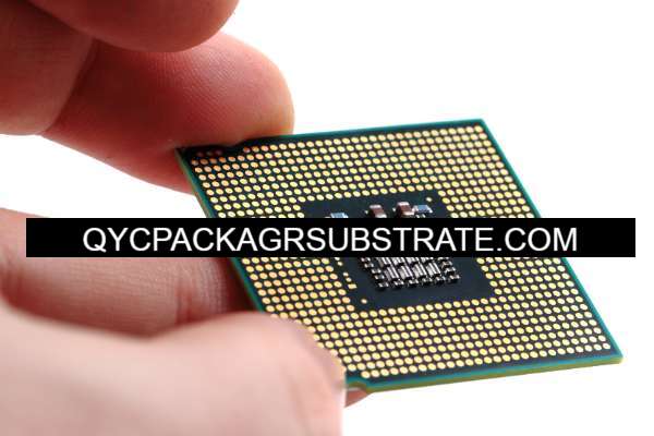
What is a WBFCLGA Substrate?
WBFCLGA (Wafer-Level Bump Flip-Chip Land Grid Array) substrate is an advanced substrate technology used for high-performance integrated circuit (IC) packaging. Its main feature is the placement of solder bumps or balls directly at the wafer level, utilizing thin-film technology to create solder balls on the silicon wafer. This technology, known as Wafer-Level Packaging (WLP), reduces unnecessary steps in the packaging process, enhances manufacturing efficiency, and provides better electrical performance.
The structure of a WBFCLGA substrate includes a silicon wafer covered with solder balls, which serve as the connection points between the IC chip and the external circuit. Compared to traditional packaging methods, such as leadframes or printed circuit board (PCB) packaging, WBFCLGA offers higher integration, smaller size, and improved electrical performance. This packaging technology is particularly suitable for applications requiring high performance and miniaturization, such as smartphones, tablets, and high-performance computing devices.
Advantages of WBFCLGA include excellent electrical performance, lower signal delay, higher thermal dissipation, and a more compact packaging design. These benefits make WBFCLGA an ideal choice for high-end IC packaging in modern electronic devices.
WBFCLGA Substrate Manufacturer
What are the WBFCLGA Substrate Design Guidelines?
WBFCLGA (Wafer-Level Bump Flip-Chip Land Grid Array) Substrate Design Guidelines
- Design Rule Specifications: Ensure adherence to precise design rules for bump pitch, pad dimensions, and alignment tolerances. The typical bump pitch ranges from 0.3 mm to 0.8 mm, depending on the application requirements.
- Thermal Management: Incorporate thermal vias and heat spreaders to manage heat dissipation effectively. Proper thermal management is crucial to prevent overheating and ensure reliable operation of the IC.
- Electrical Performance:Optimize the design for minimal signal interference and impedance control. Use high-quality materials for the substrate to maintain signal integrity and reduce parasitic effects.
- Mechanical Stability:Design for mechanical robustness to withstand stresses during handling and assembly. The substrate should provide adequate support to prevent warping or damage.
- Bump Placement: Accurate placement of solder bumps is essential for reliable electrical connections. Ensure precise alignment between the bumps and the corresponding pads on the IC and PCB.
- Pad Design: Design the land pads with appropriate dimensions and surface finishes to facilitate reliable soldering. The pad layout should support the desired solder joint quality and mechanical strength.
- Test Points:Include test points for electrical testing and verification during the manufacturing process. This allows for quality control and troubleshooting of potential issues.
- Material Selection: Choose substrate materials that offer good thermal conductivity, electrical performance, and mechanical strength. Common materials include high-quality ceramics or advanced polymers.
- Manufacturing Processes: Ensure that the design is compatible with the manufacturing processes, including wafer-level bumping, soldering, and final packaging. Collaboration with manufacturers can help in optimizing the design for production efficiency.
- Reliability Testing: Implement rigorous testing procedures to evaluate the reliability of the substrate under various environmental conditions, such as temperature cycling and humidity.
These guidelines help ensure the successful design and implementation of WBFCLGA substrates, providing high performance and reliability for advanced electronic applications.
What is the WBFCLGA Substrate Fabrication Process?
The WBFCLGA (Wafer-Level Bump Flip-Chip Land Grid Array) substrate fabrication process involves several key steps to create a high-performance, compact packaging solution for integrated circuits (ICs). Here’s an overview of the typical fabrication process:
- Wafer Preparation: Start with a silicon wafer that has been processed and tested to ensure it meets the required quality standards. The wafer is typically cleaned and inspected before further processing.
- Dielectric Layer Deposition: Deposit a dielectric material, such as silicon dioxide or a polymer layer, onto the wafer. This layer acts as an insulating barrier between the metal pads and the silicon substrate.
- Metalization: Apply a metal layer (usually copper) on top of the dielectric layer. This metal layer forms the conductive pads that will eventually connect to the solder bumps.
- Photoresist Application and Patterning: Apply a photoresist layer on the metalized wafer and use photolithography to define the patterns for the solder bump pads. The photoresist is then exposed to light through a mask and developed to create the desired pattern.
- Etching: Etch away the unwanted metal to create the exposed pads for the solder bumps. This process removes the metal in areas not protected by the photoresist.
- Solder Bump Formation: Deposit solder onto the exposed metal pads. Techniques like electroplating or stencil printing are used to form the solder bumps. The solder is then reflowed to create spherical bumps that will serve as the connection points for the IC.
- Underfill and Encapsulation: Apply an underfill material around the solder bumps to protect them and provide mechanical support. The underfill material is typically a resin that fills the gaps between the substrate and the IC, enhancing reliability and thermal performance.
- Wafer Testing and Dicing: Perform electrical and mechanical tests on the wafer to ensure that the solder bumps and pads are properly formed and functioning. After testing, the wafer is diced into individual chips.
- Final Inspection and Packaging: Inspect the diced chips for defects and ensure they meet quality standards. The chips are then packaged according to the specific application requirements, which may include mounting onto a PCB or further assembly.
- Final Testing: Conduct final testing to verify the performance and reliability of the packaged ICs. This ensures that the WBFCLGA substrate meets all required specifications and functions correctly in its intended application.
This process ensures the production of high-quality WBFCLGA substrates with excellent electrical performance and mechanical reliability, suitable for advanced electronic applications.
How do you manufacture a WBFCLGA Substrate?
Manufacturing Process for WBFCLGA (Wafer-Level Bump Flip-Chip Land Grid Array) Substrate
- Wafer Preparation: Start with a clean silicon wafer that has undergone initial processing to meet quality standards. This wafer serves as the base for further fabrication steps.
- Dielectric Layer Deposition: Apply a dielectric layer, such as silicon dioxide or a polymer, onto the wafer. This insulating layer separates the metal pads from the silicon substrate and provides electrical isolation.
- Metalization: Deposit a metal layer (typically copper) on top of the dielectric layer. This metal layer will form the conductive pads for the solder bumps. Techniques like sputtering or evaporation are commonly used for this step.
- Photoresist Application and Patterning: Coat the wafer with a photoresist material. Use photolithography to define the patterns for the solder bump pads. The photoresist is exposed to light through a mask, and then developed to reveal the desired pattern.
- Etching: Etch the metal layer to remove unwanted areas, leaving behind the metal pads that will eventually be used for solder bump connections. This step ensures the correct pattern and shape of the pads.
- Solder Bump Formation: Deposit solder onto the exposed metal pads using methods such as electroplating or stencil printing. The solder is then reflowed to form spherical bumps. These solder bumps will connect the IC to the external circuitry.
- Underfill and Encapsulation: Apply an underfill material around the solder bumps to enhance mechanical stability and thermal performance. This resin material fills the gaps between the substrate and the IC, providing additional protection and support.
- Wafer Testing and Dicing: Perform electrical testing to ensure the solder bumps and pads are correctly formed and functional. After testing, dice the wafer into individual chips using a dicing saw.
- Final Inspection and Packaging: Inspect the diced chips for defects and ensure they meet quality standards. Package the chips according to their intended application, which may involve mounting them onto a PCB or other assembly steps.
- Final Testing: Conduct comprehensive testing to verify the performance and reliability of the packaged ICs. This final step ensures that the WBFCLGA substrates meet all specifications and perform correctly in their application.
This manufacturing process produces WBFCLGA substrates that offer high performance, reliability, and compactness, suitable for advanced electronic devices.
How much should a WBFCLGA Substrate cost?
The cost of a WBFCLGA (Wafer-Level Bump Flip-Chip Land Grid Array) substrate can vary significantly depending on several factors, including:
- Size and Complexity: Larger substrates or those with more complex designs typically cost more due to increased material and processing requirements.
- Volume: Higher production volumes often lead to lower per-unit costs due to economies of scale. Conversely, smaller batch sizes may incur higher costs.
- Material Costs: The choice of materials used, such as high-quality ceramics or advanced polymers, can impact the cost. Premium materials for improved performance and reliability will increase the price.
- Manufacturing Processes: Advanced manufacturing processes, including high-precision photolithography and electroplating, can add to the cost. The complexity of the bump formation and encapsulation processes also affects pricing.
- Testing and Quality Control: Extensive testing and quality control measures contribute to the overall cost. High reliability and performance standards require rigorous testing, which can be expensive.
- Customization: Customized designs or specific requirements for particular applications can lead to additional costs. Custom tooling or unique design features add to the overall expense.
As of recent estimates, the cost of WBFCLGA substrates can range from $1 to $10 per unit for standard configurations. For specialized or high-volume applications, the cost can vary more widely. It’s best to consult with substrate manufacturers or suppliers to get accurate pricing based on your specific requirements and order volume.
What is WBFCLGA Substrate Base Material?
The base material of a WBFCLGA (Wafer-Level Bump Flip-Chip Land Grid Array) substrate plays a crucial role in determining its performance, reliability, and overall quality. The choice of base material impacts factors such as electrical conductivity, thermal management, and mechanical stability. Here are the common base materials used for WBFCLGA substrates:
- Silicon (Si): Silicon is the most commonly used base material for WBFCLGA substrates. It provides a stable platform for the fabrication of integrated circuits and is compatible with various processing techniques. Silicon substrates offer good electrical performance and are widely used due to their established manufacturing processes.
- Ceramic Materials: High-quality ceramics, such as alumina (Al2O3) or beryllium oxide (BeO), can be used as the base material for WBFCLGA substrates. Ceramics provide excellent thermal conductivity and electrical insulation, making them suitable for high-performance applications that require effective heat dissipation and minimal electrical interference.
- Polyimide and Other Organic Materials: For certain applications, organic materials such as polyimide can be used as the base material. These materials offer flexibility, good thermal stability, and are often used in applications where a thinner substrate is desirable.
- Advanced Composite Materials:In some high-end applications, advanced composite materials are used to achieve specific performance characteristics. These materials may include combinations of ceramics and polymers to optimize both mechanical properties and thermal management.
The selection of base material for a WBFCLGA substrate depends on the specific requirements of the application, including electrical performance, thermal management, and mechanical robustness. Manufacturers choose the base material based on these criteria to ensure that the final substrate meets the desired performance and reliability standards.
Which company makes WBFCLGA Substrates?
Companies Manufacturing WBFCLGA (Wafer-Level Bump Flip-Chip Land Grid Array) Substrates
The production of WBFCLGA (Wafer-Level Bump Flip-Chip Land Grid Array) substrates involves highly precise manufacturing processes and is typically handled by specialized semiconductor packaging and substrate manufacturers. Here are some well-known companies that produce WBFCLGA substrates:
- TSMC (Taiwan Semiconductor Manufacturing Company): As a leading global semiconductor manufacturer, TSMC has extensive experience in producing WBFCLGA substrates. They offer high-quality wafer-level packaging solutions suitable for various high-performance electronic applications.
- ASE Group (Advanced Semiconductor Engineering): ASE Group is a global leader in semiconductor packaging and testing, providing a range of packaging technologies, including WBFCLGA. They have extensive expertise in packaging design and manufacturing.
- GlobalFoundries: GlobalFoundries, a major semiconductor foundry, also offers WBFCLGA substrate manufacturing services. They focus on advanced packaging solutions to meet the demands of high-performance computing and consumer electronics.
- Amkor Technology: Amkor Technology is a well-known global semiconductor packaging and testing company, offering a variety of packaging technologies, including WBFCLGA. They have advanced manufacturing facilities and a highly skilled technical team.
- JCET (Jiangsu Changjiang Electronics Technology Co., Ltd.): JCET is a leading semiconductor packaging company in China, also providing WBFCLGA substrate production services. They are committed to delivering high-quality packaging solutions and hold a significant position in the domestic market.
Our company also produces WBFCLGA substrates. With advanced production facilities and technical capabilities, we provide high-quality WBFCLGA substrates to meet the demands of various high-performance electronic applications. Our manufacturing process includes:
- Wafer Preparation:We use high-quality silicon wafers, thoroughly cleaned and tested to meet quality standards.
- Dielectric Layer Deposition: We deposit dielectric materials, such as silicon dioxide or polymers, onto the wafer to provide necessary electrical insulation.
- Metalization:We apply a metal layer (e.g., copper) on the dielectric layer to form the solder bump connection points.
- Photolithography and Etching: We use photolithography to define the bump patterns and etch away excess metal to form the final bump pads.
- Solder Bump Formation: We employ advanced solder bump deposition and reflow processes to ensure accurate bump shape and placement.
- Underfill and Encapsulation: We apply underfill materials to enhance mechanical stability and thermal management, followed by final packaging and testing.
Our WBFCLGA substrates are widely used in smartphones, tablets, high-performance computing devices, and more. We are committed to providing high-performance, reliable products and offer customized services based on specific customer needs. If you require more information or have special requirements, please feel free to contact us.
What are the 7 qualities of good customer service?
Good customer service is essential for building strong relationships with clients and ensuring their satisfaction. Here are seven key qualities of effective customer service:
- Empathy: Understanding and sharing the feelings of customers is crucial. Empathetic service representatives can better address concerns, show genuine care, and build rapport with customers. This quality helps in making customers feel valued and understood.
- Patience: Customer service often involves dealing with frustrated or confused customers. Patience allows service representatives to handle inquiries and complaints calmly and effectively, providing clear and thoughtful responses without showing frustration.
- 3. Responsiveness:Quick and efficient responses to customer inquiries and issues are vital. Good customer service means addressing concerns promptly and providing timely solutions, which helps in building trust and demonstrating reliability.
- Communication Skills: Effective communication is key to good customer service. Representatives should be able to convey information clearly and concisely, listen actively, and use appropriate language and tone. This helps in ensuring that customers understand the solutions and instructions provided.
- Knowledgeability: A deep understanding of the products or services offered is essential. Knowledgeable representatives can provide accurate information, troubleshoot issues effectively, and offer valuable insights, which enhances the overall customer experience.
- Attentiveness:Paying close attention to customer needs and details is crucial. Attentive service means actively listening to customers, asking clarifying questions when needed, and ensuring that their concerns are fully addressed. This helps in delivering personalized and effective support.
- Professionalism:Maintaining a high level of professionalism in all interactions is important. This includes being courteous, respectful, and maintaining a positive attitude. Professionalism helps in creating a positive impression and building long-term customer loyalty.
These qualities collectively contribute to a positive customer service experience, fostering customer satisfaction and loyalty.
FAQs
What is a WBFCLGA Substrate?
A WBFCLGA Substrate is a high-performance substrate used in electronic packaging for mounting and connecting semiconductor chips.
What are the main design guidelines for WBFCLGA Substrates?
Design guidelines include pad layout, thermal management, signal integrity, mechanical strength, manufacturing tolerances, material selection, and testing.
How is a WBFCLGA Substrate fabricated?
The fabrication process involves material preparation, patterning, deposition, etching, bonding, testing, and packaging.
What factors influence the cost of a WBFCLGA Substrate?
Factors include substrate size, complexity, material, and quantity.
What materials are used for WBFCLGA Substrates?
Base materials typically include high-quality ceramics or composites.
Which companies produce WBFCLGA Substrates?
Many companies manufacture WBFCLGA Substrates, including our own, which specializes in producing high-quality substrates.
What are the key qualities of good customer service?
Key qualities include responsiveness, empathy, professionalism, clear communication, reliability, problem solving, and personalization.