
Wire Bonding Substrates Manufacturer
Wire Bonding Substrates Manufacturer,Wire Bonding Substrates are crucial components in semiconductor and microelectronics packaging, providing a stable platform for connecting integrated circuits (ICs) to external circuits using fine wires. These substrates, often made from materials like alumina, aluminum nitride, or organic laminates, offer excellent thermal conductivity and electrical insulation. Their precise surface finish and mechanical stability ensure reliable wire bonding processes, enhancing the performance and longevity of electronic devices. Wire bonding substrates are widely used in applications such as automotive electronics, consumer electronics, and aerospace, where dependable electrical connections and robust performance are essential for device reliability and efficiency.
What are Wire Bonding Substrates?
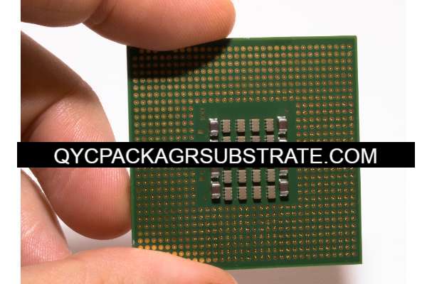
Wire bonding substrates refer to materials used in semiconductor packaging where integrated circuits (ICs) are interconnected to external circuitry using fine metallic wires. These substrates play a crucial role in ensuring the reliability and performance of electronic devices. Typically made from materials like ceramics (alumina or aluminum nitride) or organic materials (like FR4 or polyimide), wire bonding substrates provide a stable base for mounting semiconductor chips and facilitate the routing of electrical signals between the chip and the package’s external connections.
The choice of substrate material depends on various factors such as thermal management requirements, electrical performance, cost considerations, and the specific application of the electronic device. For instance, ceramic substrates are preferred for their excellent thermal conductivity and stability, making them suitable for high-power applications. Organic substrates, on the other hand, are lighter and more cost-effective, making them ideal for consumer electronics and applications where weight and cost are critical factors.
In wire bonding, the substrate must also provide mechanical support to the fine wires that connect the ICs to the package leads or terminals. The substrate material must be compatible with the wire bonding process, which involves creating precise electrical connections by thermosonic bonding or ultrasonic bonding of the wires to designated bonding pads on the semiconductor chip and the substrate.
Overall, wire bonding substrates are essential components in semiconductor packaging, enabling the efficient and reliable operation of various electronic devices across industries ranging from automotive and aerospace to telecommunications and consumer electronics.
Wire Bonding Substrates Manufacturer
What are the Wire Bonding Substrates Design Guidelines?
Design guidelines for wire bonding substrates are crucial to ensure the reliability and performance of semiconductor packages. Here are some key guidelines:
- Material Selection: Choose substrate materials based on thermal conductivity, coefficient of thermal expansion (CTE), electrical properties (dielectric constant, insulation resistance), mechanical strength, and compatibility with the wire bonding process.
- Pad Layout and Dimensions: Design bonding pad layouts with considerations for wire bonding process capabilities (e.g., pitch, pad size, spacing). Ensure adequate space between pads to accommodate the wire bonding tool and to avoid wire sweep issues.
- Pad Metallization: Use suitable metallization materials and thicknesses for bonding pads to ensure good adhesion, electrical conductivity, and reliability of wire bonds. Common materials include aluminum, gold, or alloys like aluminum-silicon (AlSi).
- Substrate Thickness and Warpage: Control substrate thickness to prevent excessive warpage during processing, which can affect wire bonding accuracy and reliability. Thicker substrates generally offer better mechanical stability but may require adjustments in bonding process parameters.
- Die Attach and Alignment: Ensure precise alignment and attachment of the semiconductor chip (die) to the substrate. Proper alignment reduces stress on wire bonds and improves electrical performance.
- Thermal Management: Incorporate features for effective heat dissipation from the semiconductor chip to the substrate and package. This may include thermal vias, thermal pads, or metal layers for improved thermal conductivity.
- Circuit Routing and Signal Integrity: Design substrate circuits to minimize signal path lengths and impedance mismatches, which can affect signal integrity. Maintain signal integrity through proper routing and ground plane placement.
- Environmental and Reliability Considerations: Design substrates to withstand environmental stresses such as temperature variations, moisture, and mechanical shocks. Consider reliability standards and qualification requirements for specific applications (e.g., automotive, aerospace).
- Assembly and Handling: Design substrates with features that facilitate assembly processes, such as pick-and-place compatibility, alignment marks, and fiducials for accurate placement during manufacturing.
- Cost and Manufacturing Feasibility: Balance substrate design considerations with cost-effectiveness and manufacturability. Optimize substrate designs to minimize material waste, process complexity, and assembly time.
By following these design guidelines, engineers can optimize wire bonding substrate designs for enhanced performance, reliability, and manufacturability of semiconductor packages across various applications and industries.
What is the Wire Bonding Substrates Fabrication Process?
The fabrication process of wire bonding substrates involves several key steps to create the base materials that will support the interconnection of semiconductor chips to external circuitry. Here’s an expanded overview of the fabrication process:
- Substrate Material Selection:The process begins with the selection of suitable substrate materials based on the specific requirements of the application. Common substrate materials include ceramics (such as alumina or aluminum nitride) and organic materials (like FR4 or polyimide). Each material offers different properties such as thermal conductivity, mechanical strength, and electrical insulation, which are critical for the performance and reliability of the final semiconductor package.
- Substrate Preparation:The selected substrate material undergoes preparation steps such as cleaning and surface treatment to ensure proper adhesion and compatibility with subsequent processing steps. Surface treatment may involve chemical etching, plasma cleaning, or mechanical polishing to achieve the required surface smoothness and cleanliness.
- Metallization:Metallization of the substrate is essential to create bonding pads and interconnects that facilitate the wire bonding process. Typically, thin layers of metals such as aluminum, gold, or alloys like aluminum-silicon (AlSi) are deposited onto the substrate surface using techniques such as sputtering, evaporation, or electroplating. The metallization process ensures good electrical conductivity and adhesion of bonding pads to the substrate.
- Photolithography and Etching:Photolithography is employed to define the pattern of bonding pads and interconnects on the substrate surface. A photoresist material is applied and exposed to ultraviolet (UV) light through a mask that contains the desired pattern. After exposure, the substrate is developed to remove the unexposed photoresist, leaving behind a patterned layer of photoresist that protects areas where metal deposition is not required. Subsequent etching processes selectively remove unprotected metal areas, defining the final shape and size of bonding pads and interconnects.
- Die Attach:Once the substrate metallization and patterning are complete, semiconductor chips (or dies) are attached to the substrate using die attach materials such as epoxy adhesives or solder pastes. Proper alignment and bonding are crucial to ensure electrical and thermal connectivity between the die and the substrate.
- Wire Bonding:Wire bonding is a critical step where fine metallic wires (typically made of gold or aluminum) are bonded between the bonding pads on the semiconductor chip and the corresponding pads on the substrate. There are two primary types of wire bonding processes: thermosonic bonding and ultrasonic bonding. These processes involve applying heat, pressure, and ultrasonic energy to create a reliable electrical connection between the wire and the bonding pad.
- Encapsulation and Packaging:After wire bonding, the semiconductor chip and wire bonds are encapsulated with protective materials such as molding compounds or epoxy resins. Encapsulation provides mechanical support, protects the wires and chip from environmental factors (such as moisture and contaminants), and enhances the overall reliability of the packaged device.
- Testing and Quality Assurance:Throughout the fabrication process, various testing and quality assurance measures are implemented to ensure the reliability and functionality of the wire bonding substrates. These tests may include electrical testing, thermal cycling tests, visual inspection, and adherence to industry standards and specifications.
- Assembly and Integration:Once fabricated and tested, the wire bonding substrates are integrated into larger electronic assemblies or systems according to specific application requirements. This may involve further assembly steps such as mounting onto printed circuit boards (PCBs), connecting to external leads or terminals, and final testing of the assembled electronic devices.
- Packaging and Shipping:The final packaged electronic devices are prepared for distribution and shipping to end-users or customers. Packaging includes protective measures to ensure that devices arrive safely and intact, ready for deployment in various applications such as consumer electronics, automotive electronics, telecommunications, and more.
By following these steps and adhering to stringent quality control measures, manufacturers can produce wire bonding substrates that meet the demanding requirements of modern semiconductor packaging, ensuring high performance, reliability, and durability of electronic devices across diverse industries.
How do you manufacture Wire Bonding Substrates?
Manufacturing wire bonding substrates involves a series of precise steps and processes to create the foundation for interconnecting semiconductor chips to external circuitry. Here’s an expanded overview of the manufacturing process:
- Substrate Material Selection:The process begins with selecting substrate materials based on specific application requirements. Common materials include ceramics like alumina (Al2O3) or aluminum nitride (AlN), known for their excellent thermal conductivity and mechanical strength. Organic materials such as FR4 (fiberglass-reinforced epoxy laminate) or polyimide are also used for their lightweight properties and flexibility.
- Substrate Preparation:Substrate preparation involves cleaning and surface treatment to ensure the substrate’s surface is free of contaminants and suitable for subsequent processing steps. Cleaning methods may include solvent cleaning, ultrasonic cleaning, or plasma cleaning. Surface treatment techniques like mechanical polishing or chemical etching may be employed to achieve the required surface smoothness and cleanliness.
- Metallization:Metallization is crucial for creating bonding pads and interconnects on the substrate surface. Typically, thin layers of metals such as aluminum, gold, or alloys like aluminum-silicon (AlSi) are deposited onto the substrate. This can be achieved through techniques such as physical vapor deposition (PVD), chemical vapor deposition (CVD), sputtering, or electroplating. The choice of metallization method depends on factors like material compatibility, deposition uniformity, and cost-effectiveness.
- Photolithography and Etching:Photolithography is used to define the pattern of bonding pads and interconnects on the substrate. A photoresist material is applied to the substrate surface and exposed to UV light through a mask containing the desired pattern. After exposure, the photoresist is developed to remove the unexposed areas, leaving behind a patterned layer that protects areas where metal deposition is not needed. Etching processes, such as wet chemical etching or dry plasma etching, are then used to selectively remove the exposed metal, defining the final shape and size of bonding pads and interconnects.
- Die Attach:Semiconductor chips (or dies) are attached to the substrate using die attach materials such as epoxy adhesives or solder pastes. The die attach process involves precise alignment of the chip to the substrate’s bonding pads. Epoxy adhesives are typically dispensed in controlled amounts, while solder pastes are often reflowed to achieve secure and reliable bonding between the chip and the substrate.
- Wire Bonding:Wire bonding is a critical process where fine metallic wires (usually gold or aluminum) are bonded between the bonding pads on the semiconductor chip and corresponding pads on the substrate. Two primary bonding methods are used: thermosonic bonding and ultrasonic bonding. These methods apply heat, pressure, and ultrasonic energy to create a metallurgical bond between the wire and the bonding pads, ensuring electrical conductivity and mechanical stability.
- Encapsulation and Packaging:After wire bonding, the semiconductor chip and wire bonds are encapsulated with protective materials such as molding compounds or epoxy resins. Encapsulation provides mechanical support, protects the wires and chip from environmental factors (such as moisture and contaminants), and enhances the overall reliability of the packaged device.
- Testing and Quality Assurance:Throughout the manufacturing process, various tests are conducted to ensure the quality and reliability of wire bonding substrates. These tests may include electrical testing, thermal cycling tests, visual inspection, and adherence to industry standards and specifications. Quality assurance measures are implemented to identify and address any defects or inconsistencies that could affect the performance of the final electronic device.
- Assembly and Integration:Once fabricated and tested, wire bonding substrates are integrated into larger electronic assemblies or systems according to specific application requirements. This may involve mounting onto printed circuit boards (PCBs), connecting to external leads or terminals, and final testing of the assembled electronic devices.
- Packaging and Shipping:The final packaged electronic devices are prepared for distribution and shipping to end-users or customers. Packaging includes protective measures to ensure that devices arrive safely and intact, ready for deployment in various applications such as consumer electronics, automotive electronics, telecommunications, and more.
By meticulously following these manufacturing steps and implementing rigorous quality control measures, manufacturers can produce high-quality wire bonding substrates that meet the stringent requirements of modern semiconductor packaging, ensuring reliability, durability, and optimal performance in diverse electronic applications.
How much should Wire Bonding Substrates cost?
The cost of wire bonding substrates can vary widely depending on several factors related to their material composition, design complexity, manufacturing process, and application requirements. Here are some key considerations that influence the cost:
- Substrate Material: The choice of substrate material significantly impacts cost. Ceramic substrates (e.g., alumina, aluminum nitride) generally cost more than organic substrates (e.g., FR4, polyimide) due to their superior thermal conductivity and mechanical properties. Specialty materials with enhanced properties (e.g., high thermal conductivity ceramics) can also increase substrate costs.
- Size and Complexity: Larger substrates or substrates with complex designs (e.g., intricate patterns of bonding pads, multiple layers) require more materials and may involve additional processing steps, which can increase manufacturing costs.
- Metallization and Surface Finish: The type of metallization (e.g., gold, aluminum, alloys) and the process used (e.g., sputtering, electroplating) affect substrate costs. Higher purity metals or thicker metallization layers can add to the cost.
- Manufacturing Process: The complexity of the manufacturing process, including photolithography, etching, die attach, wire bonding, encapsulation, and testing, influences overall production costs. More sophisticated processes or tighter tolerances may require specialized equipment and skilled labor, adding to costs.
- Volume and Scale: Economies of scale play a significant role in determining substrate costs. Larger production volumes generally lead to lower unit costs due to efficiencies in materials procurement, equipment utilization, and overhead expenses.
- Quality and Reliability Requirements: Meeting stringent quality standards and reliability requirements may necessitate additional testing, quality assurance measures, and certifications, which can impact costs.
- Market Demand and Supplier Dynamics: Market conditions, competition among suppliers, and geographic location of manufacturing facilities can also influence substrate pricing.
To provide a specific cost estimate, it would be necessary to consider detailed specifications such as substrate material type, dimensions, metallization requirements, and production volume. Generally, prices for standard wire bonding substrates can range from a few cents to several dollars per unit, with custom or specialized substrates potentially costing more depending on the factors listed above.
For accurate pricing, it’s recommended to consult with substrate manufacturers or suppliers who can provide quotes based on specific project requirements and volumes. They can also offer insights into cost-saving strategies or alternative materials that meet performance requirements while optimizing manufacturing expenses.
What is Wire Bonding Substrates base material?
Wire bonding substrates can be made from various base materials, depending on the specific requirements of the semiconductor packaging and the application. The choice of base material plays a crucial role in determining the substrate’s thermal conductivity, mechanical strength, electrical insulation properties, and overall performance. Here are some common base materials used for wire bonding substrates:
- Ceramics:
– Alumina (Al2O3): Alumina is a popular choice due to its excellent thermal conductivity, mechanical strength, and reliability. It provides good insulation properties and is suitable for high-power applications where heat dissipation is critical.
– Aluminum Nitride (AlN): Aluminum nitride offers even higher thermal conductivity than alumina, making it ideal for applications requiring superior heat dissipation. It also exhibits good electrical insulation properties and mechanical stability.
- Organic Materials:
– FR4 (Fiberglass-Reinforced Epoxy Laminate): FR4 is a commonly used organic substrate material due to its lower cost, ease of processing, and flexibility. It provides adequate electrical insulation and mechanical support for many consumer electronics applications.
– Polyimide: Polyimide substrates offer excellent flexibility, heat resistance, and chemical resistance. They are suitable for applications where lightweight, high-temperature operation, and reliability are important, such as aerospace and military electronics.
- Metal Core Substrates:
– Aluminum or Copper Core: These substrates have a metal core (usually aluminum or copper) with dielectric layers (such as FR4 or polyimide) laminated on top. They combine the thermal conductivity of metal with the electrical insulation properties of organic materials, making them suitable for applications requiring efficient heat dissipation and electrical isolation.
- Specialty Materials:
– Ceramic Composites: These include materials like aluminum oxide-titanium carbide (Al2O3-TiC) composites, which offer enhanced thermal conductivity and mechanical properties for demanding applications.
– High Thermal Conductivity Polymers: Certain polymers infused with thermally conductive fillers can be used to achieve improved heat dissipation while maintaining lightweight and cost-effectiveness.
The choice of base material depends on factors such as thermal management requirements, electrical performance needs, mechanical stability, cost considerations, and the specific environmental conditions in which the electronic device will operate. Manufacturers select the most appropriate base material and substrate design to ensure optimal performance, reliability, and cost-effectiveness for each application.
Which company makes Wire Bonding Substrates?
There are many companies worldwide that manufacture wire bonding substrates, including semiconductor packaging suppliers and specialized electronic materials companies. These companies leverage their expertise and advanced technologies to provide high-performance wire bonding substrates for various applications.
Some well-known companies manufacturing wire bonding substrates include:
- DuPont:As a globally renowned electronic materials supplier, DuPont offers various organic substrate materials such as FR4 and polyimide laminates for wire bonding applications in electronic packaging.
- Nippon Electric Glass (NEG): NEG focuses on glass and electronic materials, providing high-performance glass substrates and various ceramic substrates for high-temperature and high-frequency applications in semiconductor packaging.
- Fischer Technology: Fischer Technology specializes in manufacturing metal substrates and metal composite substrates for wire bonding and thermal management in high-power electronic packaging.
- Rogers Corporation: Rogers Corporation offers advanced thin film and ceramic substrate materials such as the RO4000 series and RO4400 series, suitable for wire bonding in high-frequency and microwave electronic packaging.
- NXP Semiconductors: As a semiconductor manufacturer, NXP Semiconductors not only provides chip-level products but also offers complementary wire bonding substrates to support their packaging solutions.
Our company also manufactures wire bonding substrates. As a company focused on electronic materials and semiconductor packaging solutions, we possess the following capabilities and strengths:
- Material Expertise: We have deep expertise in materials science and engineering, enabling us to select and optimize substrate materials suitable for various applications, including high-performance ceramics, organic substrates, and metal substrates.
- Advanced Manufacturing Technology: We invest in advanced manufacturing equipment and process technologies to precisely control the substrate manufacturing process, ensuring product quality and consistency.
- Customized Solutions: We provide customized wire bonding substrate solutions tailored to meet specific customer requirements, including design, manufacturing, and testing support.
- Quality Assurance and Reliability Testing: We strictly adhere to international quality standards and employ various reliability testing and quality control procedures to ensure that our wire bonding substrates meet technical specifications and performance requirements.
- Customer Service and Technical Support: We offer comprehensive customer service and technical support throughout the entire project lifecycle, from initial inquiry to production delivery, ensuring customer satisfaction and successful product launches.
With our expertise and commitment, our company delivers high-quality, reliable, and competitive wire bonding substrates for a wide range of electronic packaging applications, supporting our customers’ product innovation and market competitiveness.
What are the 7 qualities of good customer service?
Good customer service is characterized by several key qualities that contribute to customer satisfaction, loyalty, and positive brand reputation. Here are seven essential qualities:
- Responsiveness: Good customer service involves promptly addressing customer inquiries, concerns, and requests. This includes timely responses to emails, phone calls, and messages, ensuring customers feel valued and their issues are being addressed promptly.
- Empathy: Empathy is crucial in understanding and acknowledging the customer’s feelings, frustrations, or concerns. Customer service representatives should demonstrate empathy by listening actively, showing understanding, and providing reassurance or solutions tailored to the customer’s situation.
- Patience:Patience is essential when dealing with customers, especially in challenging or complex situations. Customer service professionals should remain calm, composed, and patient while listening to customer concerns and working through solutions, even if the customer is upset or irate.
- Clear Communication:Effective communication is key to good customer service. Customer service representatives should communicate clearly and concisely, using language that is easy to understand. They should provide accurate information, instructions, or explanations to help customers resolve issues or make informed decisions.
- Product Knowledge: Good customer service requires a thorough understanding of the company’s products or services. Customer service representatives should be knowledgeable enough to answer questions, provide recommendations, and troubleshoot problems effectively. They should stay updated on product updates, features, and policies.
- Problem-Solving Skills: Strong problem-solving skills are crucial in resolving customer issues efficiently and effectively. Customer service professionals should be able to analyze problems, identify root causes, and propose solutions that meet the customer’s needs and expectations. They should also follow up to ensure issues are fully resolved.
- Professionalism: Professionalism encompasses maintaining a positive attitude, being courteous and respectful at all times, and adhering to company policies and standards. Customer service representatives should strive to create a professional and trustworthy interaction with customers, building confidence in the company’s brand and services.
By embodying these qualities, organizations can deliver exceptional customer service experiences that foster customer loyalty, increase satisfaction, and differentiate themselves in competitive markets.
FAQs
What are wire bonding substrates?
Wire bonding substrates are materials used in semiconductor packaging to provide a foundation for mounting semiconductor chips (dies) and creating electrical connections (wire bonds) between the chip and the external leads or terminals of the package.
What materials are used to make wire bonding substrates?
Wire bonding substrates can be made from various materials including ceramics (e.g., alumina, aluminum nitride), organic materials (e.g., FR4, polyimide), metal core substrates (e.g., aluminum or copper core), and specialty materials tailored for specific thermal, electrical, or mechanical requirements.
What are the key characteristics of wire bonding substrates?
Key characteristics include thermal conductivity, electrical insulation properties, mechanical strength, compatibility with wire bonding processes, dimensional stability, and reliability in various environmental conditions.
What are the advantages of using wire bonding substrates?
Wire bonding substrates offer advantages such as efficient heat dissipation, reliable electrical connections, mechanical support for semiconductor chips, flexibility in design and material selection, and suitability for a wide range of applications including consumer electronics, automotive, aerospace, and telecommunications.
What types of wire bonding processes are compatible with these substrates?
Wire bonding substrates are compatible with various wire bonding processes including ball bonding and wedge bonding techniques. These processes use fine metallic wires (e.g., gold or aluminum) to create electrical connections between the bonding pads on the semiconductor chip and the substrate.
How are wire bonding substrates manufactured?
The manufacturing process typically involves substrate material selection, preparation (cleaning and surface treatment), metallization (depositing metal layers on the substrate), photolithography and etching (defining bonding pad patterns), die attach (attaching semiconductor chips), wire bonding (creating wire bonds), encapsulation (protective coating), testing, and final packaging.
What factors should be considered when selecting wire bonding substrates?
Factors to consider include thermal management requirements, electrical performance specifications, mechanical stability, compatibility with assembly processes, environmental durability, cost-effectiveness, and specific application needs (e.g., high-frequency, high-power, or miniaturized electronics).