
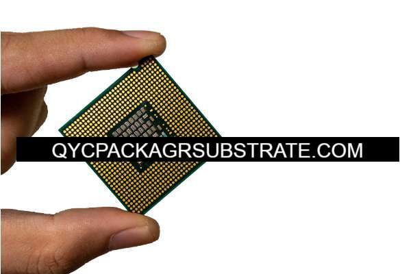
What is WLP Package Substrate?
Professional WLP Package Substrate Supplier, and WLP Package Service. Advanced production equipment and professional production team. we produce WLP substrates from 2 layer to 20 layers.
WLP stands for “Wafer-Level Packaging,” which is a technology used in semiconductor manufacturing to package integrated circuits (ICs) at the wafer level rather than the traditional method of packaging individual ICs after they have been diced from the wafer.
The WLP process involves creating the packaging structures directly on the wafer itself before the individual ICs are separated. This offers several advantages such as reduced size, improved performance, and lower cost compared to traditional packaging methods.
The package substrate in WLP refers to the material layer or layers that provide structural support and electrical connections for the integrated circuits within the package. The substrate typically consists of a thin layer of material such as silicon or glass with patterned metal traces that connect the ICs to the external leads or bumps. These substrates are designed to be extremely thin to minimize the overall package size and enable high-density integration of ICs.
Overall, WLP technology and package substrates play a crucial role in enabling the miniaturization and increased functionality of electronic devices such as smartphones, tablets, and other portable electronics.
WLP Package Substrate
What are the functions of WLP Package Substrate?
The functions of WLP package substrate include:
Structural support: The package substrate provides the necessary structural support for integrated circuits (ICs), protecting ICs from physical damage and environmental effects.
Electrical connections: The metal trace patterns on the package substrate provide electrical connections between ICs and external leads or bumps, allowing ICs to communicate and interact with other components or external systems.
Heat dissipation: The package substrate helps to conduct the heat generated by ICs to the external environment, maintaining the stable operating temperature of ICs and preventing overheating damage.
Signal transmission: Through the traces on the package substrate, signal transmission between ICs as well as between ICs and external devices, including data transmission, timing signals, and control signals, can be achieved.
Package sealing: The package substrate can serve as a sealing layer at the bottom of the package, preventing dust, moisture, and other contaminants from entering the package interior, protecting ICs from environmental damage.
In summary, WLP package substrate plays a crucial role in protection, connection, heat dissipation, and signal transmission, serving as an essential component for achieving high-performance, high-reliability integrated circuit packaging.
What are the different types of WLP Package Substrate?
There are several types of WLP (Wafer-Level Packaging) package substrates, each with its own characteristics and applications. Some common types include:
Fan-Out WLP (FO-WLP): In FO-WLP, the integrated circuits (ICs) are redistributed over a larger area on the substrate, allowing for more input/output (I/O) connections and greater flexibility in routing. This type of WLP is suitable for applications requiring high I/O density and heterogeneous integration.
Fan-In WLP (FI-WLP): In FI-WLP, the ICs are placed closer together on the substrate, with the interconnects routed inward toward the center of the package. FI-WLP is typically used for applications requiring smaller package sizes and higher integration density.
Chip-on-Wafer (CoW): CoW involves placing multiple ICs directly on the wafer surface and then packaging them together using WLP techniques. This approach enables efficient use of space and facilitates the integration of multiple functions on a single chip.
Wafer-Level Chip-Scale Package (WLCSP): WLCSP is a type of WLP where the package size is minimized to be very close to the size of the IC itself, resulting in a compact form factor suitable for space-constrained applications such as mobile devices.
Through-Silicon Via (TSV) WLP: TSV WLP involves the integration of vertical interconnects (vias) through the silicon substrate, enabling high-density connections between multiple layers of ICs. TSV WLP is used for advanced packaging applications such as 3D integration and stacking.
Embedded Wafer-Level Ball Grid Array (eWLB): eWLB is a type of WLP where the ICs are embedded within a molded compound directly on the wafer surface, providing protection and interconnectivity. eWLB offers advantages such as improved reliability and thermal performance.
These are some of the common types of WLP package substrates, each offering unique features suited to specific application requirements.
What is the relationship between WLP Package Substrate and IC packaging?
The relationship between WLP (Wafer-Level Packaging) package substrate and IC (Integrated Circuit) packaging is very close, as the package substrate is a critical component of the overall IC packaging process.
Integration of ICs onto Substrate: In WLP, the ICs are typically integrated onto the package substrate directly at the wafer level. This means that the package substrate serves as the foundation upon which the ICs are mounted and interconnected.
Electrical Connections: The package substrate provides the electrical connections between the ICs and the external world. It contains metal traces or interconnects that connect the pads on the ICs to the package’s external pins or bumps, facilitating communication and power transfer.
Protection and Support: The package substrate offers structural support and protection for the ICs. It shields the ICs from physical damage, moisture, and contaminants while also providing mechanical stability to the overall package.
Thermal Management: The package substrate plays a role in thermal management by helping to dissipate heat generated by the ICs during operation. Heat-conductive materials and designs may be incorporated into the substrate to enhance thermal performance.
Form Factor and Size: The type and design of the package substrate influence the form factor and size of the final IC package. Different substrate technologies, such as fan-out or fan-in, allow for variations in package size, density, and I/O configurations to meet specific application requirements.
Overall, the package substrate is an essential element in IC packaging, serving as the platform for integrating, interconnecting, and protecting the ICs, while also influencing the performance, size, and reliability of the final packaged device.
How does WLP Package Substrate differ from PCB?
WLP (Wafer-Level Packaging) package substrate and PCB (Printed Circuit Board) are both essential components in electronic systems, but they serve different purposes and have distinct characteristics:
Integration Level: WLP package substrate is typically used for packaging individual integrated circuits (ICs) directly at the wafer level, before they are diced into individual chips. PCBs, on the other hand, are used to interconnect multiple electronic components, including ICs, resistors, capacitors, and connectors, into a complete electronic system.
Component Mounting: In WLP, the ICs are mounted directly onto the substrate surface, with their active components facing upward. In contrast, on a PCB, components are mounted on the surface or inserted into pre-drilled holes and soldered onto the copper traces.
Interconnects: The package substrate in WLP typically contains metal traces or interconnects that connect the IC pads to external leads or bumps. In PCBs, the interconnects are formed by copper traces that are etched onto the substrate surface and connected to pads or vias.
Size and Form Factor: WLP package substrates are designed to be compact and closely matched to the size of the ICs they package, resulting in smaller overall package sizes. PCBs can vary widely in size and shape, depending on the complexity of the electronic system they are used in.
Application: WLP package substrates are commonly used in high-performance and space-constrained applications such as mobile devices, wearables, and automotive electronics. PCBs are used in a wide range of electronic systems, including computers, consumer electronics, industrial equipment, and telecommunications.
Overall, while both WLP package substrates and PCBs play crucial roles in electronic systems, they serve different functions and are designed for different levels of integration and application requirements.
What are the structure and production technology of WLP Package Substrate?
The structure and production technology of WLP (Wafer-Level Packaging) package substrate can vary depending on the specific type and design requirements. However, a general overview of the structure and production process typically involves the following steps:
Substrate Material Selection: The substrate material is chosen based on factors such as thermal conductivity, electrical properties, mechanical strength, and cost. Common substrate materials include silicon, glass, organic substrates (e.g., laminates or build-up films), and ceramics.
Wafer Preparation: The selected substrate material is processed into wafers of appropriate size and thickness. For silicon substrates, this may involve slicing silicon ingots into thin wafers and polishing them to achieve a smooth surface.
Metallization: Metal layers are deposited onto the substrate surface to form the interconnects and bonding pads. Techniques such as physical vapor deposition (PVD) or chemical vapor deposition (CVD) may be used to deposit metals such as aluminum, copper, or gold.
Patterning: Photolithography or other patterning techniques are used to define the desired patterns for the interconnects, bonding pads, and other features on the substrate surface. A photoresist layer is applied, exposed to UV light through a photomask, and then developed to transfer the pattern onto the metal layers.
Etching: The exposed metal regions are selectively etched away using wet or dry etching processes, leaving behind the desired metal interconnects and patterns.
Dielectric Deposition: Dielectric materials such as silicon dioxide (SiO2) or polyimide are deposited onto the substrate surface to insulate the metal interconnects and provide additional structural support.
Via Formation: Vias are formed in the dielectric layers to provide vertical connections between different metal layers. Techniques such as laser drilling or plasma etching may be used to create vias with precise dimensions.
Surface Finish: The substrate surface may be coated with a thin layer of metal (e.g., solder or gold) to improve solderability or provide a surface for wire bonding.
Testing and Inspection: The finished substrate undergoes rigorous testing and inspection to ensure that it meets the required electrical and mechanical specifications.
Assembly and Packaging: After testing, the substrate is ready for assembly with the integrated circuits (ICs) and other components. This may involve processes such as die attach, wire bonding, flip-chip bonding, or encapsulation, depending on the specific packaging requirements.
Overall, the production technology of WLP package substrates involves a series of sophisticated processes to create precise patterns, interconnects, and structures on the substrate surface, enabling the integration and packaging of ICs at the wafer level.
Frequently Asked Questions (FAQs)
What is WLP package substrate?
WLP package substrate refers to the material layer or layers that provide structural support and electrical connections for integrated circuits (ICs) in wafer-level packaging. It is the foundation upon which ICs are mounted and interconnected at the wafer level before being separated into individual chips.
What are the advantages of WLP package substrates?
Some advantages of WLP package substrates include smaller package sizes, improved performance, higher integration density, reduced cost, and enhanced thermal performance compared to traditional packaging methods.
What are the different types of WLP package substrates?
Common types of WLP package substrates include fan-out WLP (FO-WLP), fan-in WLP (FI-WLP), chip-on-wafer (CoW), wafer-level chip-scale package (WLCSP), through-silicon via (TSV) WLP, and embedded wafer-level ball grid array (eWLB).
How is WLP package substrate different from PCB?
While both WLP package substrates and PCBs (Printed Circuit Boards) are essential components in electronic systems, they serve different purposes. WLP package substrates are used for packaging individual ICs at the wafer level, providing structural support and electrical connections, while PCBs are used to interconnect multiple electronic components into a complete system.
What is the production process for WLP package substrates?
The production process for WLP package substrates involves steps such as substrate material selection, wafer preparation, metallization, patterning, etching, dielectric deposition, via formation, surface finish, testing, and assembly. These processes are used to create precise patterns, interconnects, and structures on the substrate surface to enable the integration and packaging of ICs at the wafer level.
Conclusion
In conclusion, WLP (Wafer-Level Packaging) package substrates play a crucial role in the semiconductor industry by providing structural support and electrical connections for integrated circuits (ICs) at the wafer level. These substrates enable the integration and packaging of ICs in a compact and efficient manner, offering advantages such as smaller package sizes, improved performance, higher integration density, and enhanced thermal performance.
Various types of WLP package substrates, including fan-out WLP (FO-WLP), fan-in WLP (FI-WLP), chip-on-wafer (CoW), wafer-level chip-scale package (WLCSP), through-silicon via (TSV) WLP, and embedded wafer-level ball grid array (eWLB), cater to different application requirements and packaging needs.
The production process for WLP package substrates involves a series of sophisticated steps, including substrate material selection, wafer preparation, metallization, patterning, etching, dielectric deposition, via formation, surface finish, testing, and assembly. These processes are essential for creating precise patterns, interconnects, and structures on the substrate surface, ensuring the reliability and performance of the packaged ICs.
Overall, WLP package substrates represent an innovative and efficient packaging solution that contributes to the advancement of electronic devices, enabling smaller, more powerful, and more reliable electronic systems.