
3D Ceramic Packages Substrate manufacturing
3D Ceramic Packages Substrate manufacturing, Advanced 3D production technology, professional team, fast delivery, stable quality. We produce various ceramic substrates and PCBs.
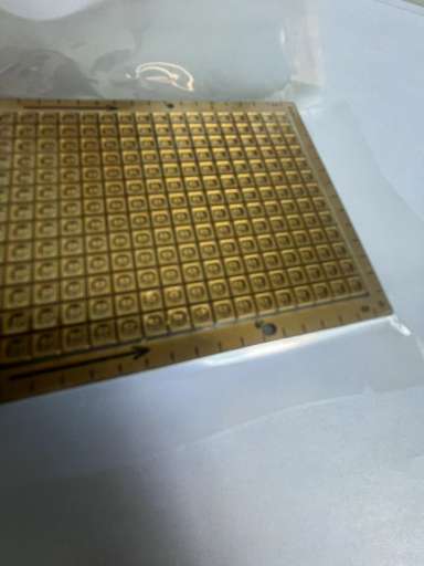
3D Ceramic Packages Substrates represent a cutting-edge advancement in semiconductor packaging technology. These substrates are engineered with multiple layers of ceramic material, intricately designed to accommodate complex circuitry and interconnects in a three-dimensional structure. By leveraging the exceptional thermal conductivity, electrical insulation, and mechanical strength of ceramic materials like alumina (Al2O3) or aluminum nitride (AlN), these substrates offer unparalleled performance and reliability for semiconductor devices. Their compact size, high integration capability, and efficient heat dissipation make them ideal for applications demanding superior performance, such as high-performance microprocessors, memory chips, and system-on-chip (SoC) designs. Through innovative manufacturing processes and meticulous design considerations, 3D ceramic package substrates empower the next generation of electronic devices, enabling advancements in computing, communications, and beyond.
What is a 3D Ceramic Packages Substrate?
3D Ceramic Packages Substrate manufacturing. the Package Substrate will be made with Showa Denko and Ajinomoto High speed materials.or other types high speed materials and high frequency materials.
A 3D ceramic package substrate refers to a type of packaging technology used in the semiconductor industry, particularly in integrated circuit (IC) packaging.
Traditionally, semiconductor devices are packaged using substrates made of materials like ceramic or organic materials. These substrates provide mechanical support for the semiconductor die (the actual integrated circuit), as well as electrical connections between the die and the external circuitry.
A 3D ceramic package substrate takes this concept further by incorporating multiple layers of circuitry and interconnects within the substrate itself. This allows for more efficient use of space and enables the integration of additional functionality, such as passive components like capacitors or inductors, within the package itself.
By stacking multiple layers of circuitry and interconnects, 3D ceramic package substrates can achieve higher levels of integration, improved performance, and increased functionality compared to traditional packaging techniques. These substrates are commonly used in advanced semiconductor devices, such as high-performance microprocessors, memory chips, and system-on-chip (SoC) designs, where compact size, high performance, and reliability are critical requirements.
What are the 3D Ceramic Packages Substrate Design Guidelines?
Design guidelines for 3D ceramic package substrates can vary depending on specific requirements, technology nodes, and application scenarios. However, some common design principles and guidelines may include:
- Layer Stackup Design: Determine the number of layers needed for the substrate based on the complexity of the design and the required functionality. Consider factors such as signal integrity, power distribution, and thermal management when designing the layer stackup.
- Material Selection: Choose appropriate ceramic materials with suitable electrical, thermal, and mechanical properties for the intended application. Consider factors such as dielectric constant, coefficient of thermal expansion (CTE), and thermal conductivity.
- Interconnect Design: Design the interconnects (traces, vias, and through-holes) to provide efficient electrical connections between different layers and components on the substrate. Optimize trace widths, spacing, and via placement to minimize signal loss, crosstalk, and impedance mismatches.
- Power Delivery Network (PDN) Design: Design the power delivery network to ensure stable and efficient distribution of power to the semiconductor devices on the substrate. Use techniques such as power planes, decoupling capacitors, and optimized routing to minimize voltage drops and noise.
- Thermal Management: Implement thermal vias, metal layers, and other techniques to efficiently dissipate heat generated by the semiconductor devices and maintain optimal operating temperatures. Ensure adequate thermal conductivity and heat dissipation paths within the substrate.
- Signal Integrity (SI) and Electromagnetic Compatibility (EMC): Perform SI and EMC analysis to ensure signal integrity and compliance with electromagnetic interference (EMI) standards. Consider factors such as impedance control, signal routing, and shielding to minimize noise and interference.
- Package Integration: Integrate additional components such as passive devices (e.g., capacitors, inductors) and embedded dies within the substrate to achieve higher levels of integration and functionality. Optimize the placement and routing of integrated components to minimize parasitic effects and optimize performance.
- Reliability and Manufacturing Considerations: Design the substrate to meet reliability requirements and facilitate manufacturability. Consider factors such as solder joint reliability, warpage control, and compatibility with assembly processes.
- Testing and Characterization: Develop test methodologies and characterization techniques to validate the performance and reliability of the substrate design. Conduct electrical, thermal, and mechanical testing to ensure compliance with specifications and standards.
- Design for Cost: Optimize the substrate design for cost-effectiveness by considering factors such as material costs, manufacturing complexity, and assembly requirements. Balance performance, functionality, and cost considerations to achieve the desired balance for the target application.
These guidelines provide a framework for designing 3D ceramic package substrates that meet the performance, reliability, and manufacturability requirements of advanced semiconductor devices. Designers should adapt and refine these guidelines based on specific project requirements and technology constraints.
3D Ceramic Packages Substrate
What is the 3D Ceramic Packages Substrate Fabrication Process?
The fabrication process for 3D ceramic package substrates involves several steps, including substrate preparation, layer buildup, patterning, metallization, bonding, and finishing. Here’s an overview of the typical fabrication process:
- Substrate Preparation:
– Start with a ceramic substrate material, such as alumina (Al2O3) or aluminum nitride (AlN), in the form of sheets or panels.
– Clean the substrate surface to remove any contaminants or impurities that could affect subsequent processing steps.
- Layer Buildup:
– Apply ceramic green tape or paste onto the substrate surface to build up multiple layers. These layers may contain conductive traces, vias, and insulating materials.
– Alternatively, utilize a co-firing process where layers of green tape are stacked, and then the entire assembly is fired in a furnace to sinter the layers together.
- Patterning:
– Use photolithography or other patterning techniques to define the desired circuit patterns on each layer. This involves applying a photoresist, exposing it to UV light through a mask, developing the pattern, and etching away unwanted material.
- Metallization:
– Deposit metal layers, typically through techniques such as sputtering or electroplating, to create conductive traces, pads, and vias. Common metals used for metallization include copper, gold, and silver.
– Etch away excess metal using chemical etchants or plasma etching to define the desired conductive features.
- Bonding:
– If the substrate requires multiple layers to be bonded together, use techniques such as adhesive bonding or direct bonding to laminate the layers.
– For 3D integration, bonding may also involve attaching additional components or dies onto the substrate surface or within the substrate layers.
- Finishing:
– Perform any necessary finishing processes, such as planarization, surface polishing, or coating, to ensure the substrate’s surface is smooth and free of defects.
– Optionally, add protective coatings or encapsulants to enhance the substrate’s mechanical strength, thermal performance, and reliability.
- Testing and Quality Control:
– Conduct electrical, mechanical, and thermal testing to verify the substrate’s performance and quality.
– Inspect the substrate for defects, such as cracks, voids, or delaminations, and ensure compliance with specifications and standards.
- Packaging and Assembly:
– Once the substrate fabrication is complete and validated, it can be incorporated into the overall semiconductor package assembly process.
– This may involve attaching semiconductor dies, wire bonding or flip-chip bonding, encapsulation, and final testing before the packaged device is ready for deployment.
The specific details of the fabrication process may vary depending on factors such as the substrate material, design complexity, and manufacturing capabilities. Additionally, advancements in technology and materials may lead to variations or improvements in the fabrication techniques used for 3D ceramic package substrates.
How do you manufacture a 3D Ceramic Packages Substrate?
Manufacturing a 3D ceramic package substrate involves a series of complex processes aimed at building up multiple layers of ceramic material, patterning conductive traces and vias, metallizing the layers, bonding the layers together, and finishing the substrate to meet desired specifications. Here’s a detailed outline of the manufacturing process:
- Substrate Preparation:
– Start with ceramic substrate material in the form of sheets or panels. Common materials include alumina (Al2O3) or aluminum nitride (AlN).
– Clean the substrate surface thoroughly to remove any contaminants that could affect subsequent processing steps.
- Layer Buildup:
– Apply layers of ceramic green tape or paste onto the substrate surface. These layers will form the basis for building up the substrate’s structure.
– Alternatively, utilize a co-firing process where layers of green tape are stacked, and then the entire assembly is fired in a furnace to sinter the layers together.
- Patterning:
– Use photolithography or other patterning techniques to define the desired circuit patterns on each layer. This involves applying a photoresist, exposing it to UV light through a mask, developing the pattern, and etching away unwanted material to reveal the conductive traces and vias.
- Metallization:
– Deposit metal layers onto the substrate’s surface to form the conductive traces, pads, and vias. Common metals used for metallization include copper, gold, and silver.
– The metal layers can be deposited through techniques such as sputtering, electroplating, or chemical vapor deposition (CVD).
- Bonding:
– If the substrate requires multiple layers to be bonded together, use techniques such as adhesive bonding or direct bonding to laminate the layers.
– For 3D integration, bonding may also involve attaching additional components or semiconductor dies onto the substrate surface or within the substrate layers.
- Finishing:
– Perform finishing processes such as planarization, surface polishing, or coating to ensure the substrate’s surface is smooth and free of defects.
– Optionally, add protective coatings or encapsulants to enhance the substrate’s mechanical strength, thermal performance, and reliability.
- Testing and Quality Control:
– Conduct electrical, mechanical, and thermal testing to verify the substrate’s performance and quality.
– Inspect the substrate for defects, such as cracks, voids, or delaminations, and ensure compliance with specifications and standards.
- Packaging and Assembly:
– Once the substrate manufacturing is complete and validated, it can be incorporated into the overall semiconductor package assembly process.
– This may involve attaching semiconductor dies, wire bonding or flip-chip bonding, encapsulation, and final testing before the packaged device is ready for deployment.
Throughout the manufacturing process, strict quality control measures are essential to ensure that the 3D ceramic package substrate meets the required specifications for performance, reliability, and functionality. Additionally, advancements in technology and materials may lead to refinements or innovations in the manufacturing techniques used for these substrates.
How much should a 3D Ceramic Packages Substrate cost?
The cost of a 3D ceramic package substrate can vary significantly depending on various factors such as:
- Material Cost: The cost of the ceramic material used for the substrate can vary based on factors such as material purity, quality, and availability. Materials like alumina (Al2O3) or aluminum nitride (AlN) are commonly used, and their costs can fluctuate based on market conditions.
- Manufacturing Complexity: The complexity of the substrate design, including the number of layers, the density of interconnects, and the integration of additional components, can impact manufacturing costs. More complex designs often require advanced fabrication techniques and equipment, which can increase production costs.
- Fabrication Process: The specific fabrication processes involved in manufacturing the substrate, such as layer buildup, patterning, metallization, bonding, and finishing, contribute to the overall cost. Processes that require specialized equipment or expertise may incur higher costs.
- Quality and Reliability Requirements: Meeting stringent quality and reliability standards may necessitate additional testing, inspection, and quality control measures, which can add to the manufacturing cost.
- Volume and Scale: Economies of scale can significantly impact the cost of manufacturing. Larger production volumes generally lead to lower per-unit costs due to efficiencies in production, materials procurement, and overhead expenses.
- Customization and Special Features: Customized substrates with specific features or functionalities may incur higher costs compared to standard designs. Additional features such as embedded components or specialized coatings can also contribute to the overall cost.
- Supplier and Geographic Factors: The choice of supplier and geographic location can influence costs due to differences in labor costs, overhead expenses, and supply chain logistics.
Given these factors, it’s challenging to provide a specific cost estimate for a 3D ceramic package substrate without detailed information about the design specifications, manufacturing processes, and market conditions. However, 3D ceramic package substrates are typically a significant component cost within semiconductor packaging solutions and can range from several hundred to several thousand dollars per substrate, depending on the complexity and volume of production.
What is 3D Ceramic Packages Substrate base material?
The base material for a 3D ceramic package substrate is typically a ceramic material chosen for its electrical, thermal, and mechanical properties. Two common ceramic materials used as base materials for 3D ceramic package substrates are:
- Alumina (Al2O3):
– Alumina ceramic is a widely used material in semiconductor packaging due to its excellent thermal conductivity, high electrical insulation properties, and mechanical strength.
– It is relatively cost-effective compared to other ceramic materials and offers good compatibility with semiconductor manufacturing processes.
– Alumina substrates are suitable for applications requiring moderate to high power handling capabilities and thermal dissipation.
- Aluminum Nitride (AlN):
– Aluminum nitride ceramic offers superior thermal conductivity compared to alumina, making it ideal for applications requiring efficient heat dissipation.
– AlN substrates also exhibit excellent electrical insulation properties and can withstand high operating temperatures.
– Although more expensive than alumina, aluminum nitride is preferred for high-power and high-frequency applications where thermal management is critical.
These ceramic materials serve as the foundation for building up the multiple layers of the substrate through processes such as layer deposition, patterning, metallization, and bonding. The choice between alumina and aluminum nitride as the base material depends on factors such as thermal requirements, electrical performance, cost considerations, and specific application needs. Other advanced ceramic materials may also be used for specialized applications requiring unique properties.
Which company makes 3D Ceramic Packages Substrates?
One company that manufactures 3D ceramic package substrates is Kyocera Corporation. Kyocera is a multinational electronics and ceramics manufacturer headquartered in Japan. They produce a wide range of ceramic products, including substrates used in semiconductor packaging.
Kyocera’s 3D ceramic package substrates are known for their high quality, reliability, and advanced technology. These substrates are designed to meet the demanding requirements of modern semiconductor devices, offering excellent thermal management, electrical performance, and integration capabilities.
Our company, on the other hand, is a leading manufacturer in the field of electronic components and materials. We specialize in the design and production of advanced ceramic substrates, including 3D ceramic package substrates. With state-of-the-art manufacturing facilities and a team of experienced engineers, we have the expertise and capabilities to produce high-quality substrates tailored to our customers’ specific requirements.
Our 3D ceramic package substrates are manufactured using cutting-edge fabrication processes and materials, ensuring optimal performance and reliability for semiconductor packaging applications. We prioritize customer satisfaction and strive to exceed expectations through continuous innovation, quality assurance, and responsive customer support.
By leveraging our expertise in ceramic materials and semiconductor packaging technology, we are able to deliver reliable and cost-effective solutions that meet the evolving needs of our customers in the electronics industry. With our commitment to excellence and customer-centric approach, we are confident in our ability to provide superior 3D ceramic package substrates that drive innovation and enable the next generation of electronic devices.
What are the 7 qualities of good customer service?
Good customer service is essential for building strong relationships with customers and fostering loyalty. Here are seven qualities that characterize good customer service:
- Responsiveness: Good customer service involves being prompt and proactive in addressing customer inquiries, concerns, and requests. Responding to customer needs in a timely manner demonstrates attentiveness and a commitment to customer satisfaction.
- Empathy: Empathy is the ability to understand and relate to customers’ feelings, perspectives, and experiences. Good customer service representatives listen actively, show genuine concern for customers’ issues, and strive to put themselves in the customer’s shoes to provide personalized assistance.
- Clarity and Communication Skills: Effective communication is crucial in customer service. Good customer service representatives communicate clearly, using language that is easy to understand, and provide accurate information to address customer inquiries or resolve issues. They also actively listen to customers, ask clarifying questions, and confirm understanding to ensure effective communication.
- Problem-Solving Skills: Good customer service involves being resourceful and proactive in resolving customer problems or issues. Customer service representatives should possess strong problem-solving skills, the ability to think critically, and the initiative to explore alternative solutions to meet customers’ needs.
- Professionalism: Professionalism encompasses attributes such as courtesy, respect, and integrity in customer interactions. Good customer service representatives maintain a positive and professional demeanor, even in challenging situations, and treat customers with dignity and respect at all times.
- Product Knowledge: Having a thorough understanding of the products or services offered allows customer service representatives to provide accurate information, address customer inquiries effectively, and offer helpful recommendations or solutions. Good customer service requires ongoing training and development to ensure representatives are knowledgeable about the products or services they support.
- Follow-Up and Accountability: Good customer service extends beyond the initial interaction. It involves following up with customers to ensure their needs have been met satisfactorily and addressing any additional concerns or feedback they may have. Additionally, good customer service representatives take ownership of customer issues, follow through on commitments, and take accountability for resolving problems to the best of their ability.
By embodying these qualities, organizations can deliver exceptional customer service experiences that build trust, loyalty, and long-term relationships with their customers.
FAQs (Frequently Asked Questions)
What is a 3D ceramic package substrate?
A 3D ceramic package substrate is a type of packaging technology used in the semiconductor industry. It involves stacking multiple layers of ceramic material with embedded circuitry and interconnects to create a three-dimensional structure for mounting and connecting semiconductor devices.
What are the advantages of 3D ceramic package substrates?
3D ceramic package substrates offer several advantages, including higher levels of integration, improved thermal management, reduced footprint, enhanced electrical performance, and increased reliability compared to traditional packaging techniques.
What materials are used in 3D ceramic package substrates?
Common materials used in 3D ceramic package substrates include alumina (Al2O3) and aluminum nitride (AlN). These materials offer excellent thermal conductivity, electrical insulation, and mechanical strength, making them well-suited for semiconductor packaging applications.
What are the applications of 3D ceramic package substrates?
3D ceramic package substrates are used in various semiconductor devices, including microprocessors, memory chips, system-on-chip (SoC) designs, sensors, and high-frequency RF modules. They are particularly beneficial in applications requiring compact size, high performance, and reliability.
How are 3D ceramic package substrates manufactured?
The manufacturing process for 3D ceramic package substrates involves layer buildup, patterning, metallization, bonding, and finishing. It typically includes processes such as screen printing, photolithography, sintering, and metal deposition to create the multi-layered structure with embedded circuitry and interconnects.
What considerations should be made when designing 3D ceramic package substrates?
When designing 3D ceramic package substrates, factors such as layer stackup design, material selection, interconnect design, power delivery network (PDN) design, thermal management, signal integrity (SI), electromagnetic compatibility (EMC), reliability, and manufacturing considerations should be taken into account.
Suppliers of 3D ceramic package substrates include semiconductor packaging companies, ceramic material manufacturers, and specialized electronic component suppliers. Researching online or contacting industry associations can help identify potential suppliers for specific requirements.