
Advanced Glass Package Substrates Manufacturer
Advanced Glass Package Substrates Manufacturer and package substrate Manufacturer. We use advanced Msap and Sap technology, High multilayer interconnection substrates from 4 to 18 layers,
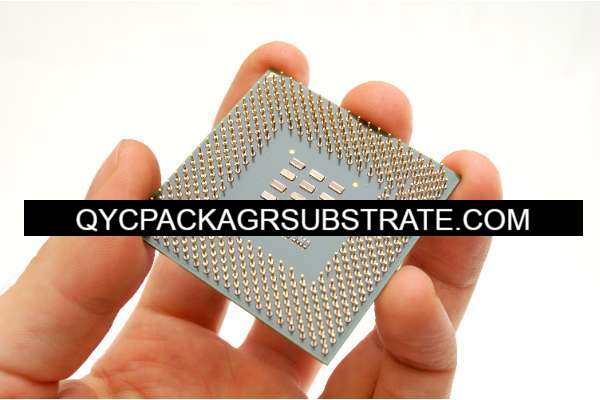
Advanced Glass Package Substrates (AGPS) are cutting-edge substrates crafted from specialized glass materials, meticulously engineered to meet the stringent demands of modern semiconductor packaging. These substrates serve as the foundation for mounting and interconnecting semiconductor chips within electronic devices, offering a myriad of advantages over traditional materials. AGPS boasts superior thermal conductivity, ensuring efficient heat dissipation and enhancing device reliability. Their exceptional electrical properties facilitate high-speed data transmission with minimal signal loss, crucial for today’s fast-paced applications. Moreover, AGPS enables miniaturization, allowing for sleeker device designs without compromising performance. The manufacturing process involves precise thin-film deposition, intricate patterning, and stringent quality control measures to ensure consistency and reliability. From smartphones and wearables to automotive electronics and high-performance computing systems, AGPS plays a pivotal role in powering the next generation of electronic devices, delivering unparalleled performance, reliability, and efficiency.
What is an Advanced Glass Package Substrate?
An Advanced Glass Package Substrate (AGPS) is a cutting-edge technology used in electronics manufacturing, particularly in semiconductor packaging. It refers to a substrate made of glass that provides a robust and high-performance platform for mounting and interconnecting semiconductor chips in various electronic devices.
AGPS offers several advantages over traditional substrates like silicon or organic materials. Firstly, it provides better thermal conductivity, which helps dissipate heat generated by the semiconductor components more efficiently, thereby improving the overall reliability and longevity of the device. Secondly, AGPS offers superior electrical properties, such as lower signal loss and improved signal integrity, leading to better performance in high-speed applications like data transmission.
Additionally, AGPS substrates can be manufactured with finer feature sizes and tighter tolerances, allowing for the integration of more complex circuitry in a smaller footprint. This miniaturization enables the development of sleeker and more compact electronic devices, which is particularly important in industries like mobile phones, wearables, and IoT devices where size and weight are critical factors.
Furthermore, AGPS technology facilitates the implementation of advanced packaging techniques such as fan-out wafer-level packaging (FOWLP) and system-in-package (SiP), which enable higher levels of integration and functionality in electronic devices.
Overall, AGPS represents a significant advancement in semiconductor packaging technology, offering improved performance, reliability, miniaturization, and integration capabilities compared to conventional substrate materials. Its adoption is expected to continue growing as demand for smaller, faster, and more efficient electronic devices continues to rise.
Advanced Glass Package Substrates Manufacturer
What are the Advanced Glass Package Substrate Design Guidelines?
Design guidelines for Advanced Glass Package Substrates (AGPS) are crucial for ensuring the optimal performance, reliability, and manufacturability of electronic devices. While specific guidelines may vary depending on the manufacturer and application, here are some common considerations:
- Thermal Management: AGPS design should incorporate effective thermal management techniques to dissipate heat generated by semiconductor components. This includes the placement of thermal vias, heat spreaders, and thermal pads to enhance heat transfer away from the device.
- Signal Integrity:Maintaining signal integrity is essential for high-speed data transmission and electrical performance. Design guidelines often include recommendations for controlled impedance traces, signal routing, and minimizing signal crosstalk to reduce electromagnetic interference (EMI) and ensure reliable signal transmission.
- Electrical Performance:AGPS designs should meet specified electrical performance requirements, such as impedance matching, power delivery, and voltage regulation. Design guidelines may include recommendations for power distribution network (PDN) design, decoupling capacitor placement, and signal/power integrity analysis to optimize electrical performance.
- Mechanical Integrity: Mechanical robustness is critical to withstand environmental stresses and ensure long-term reliability. Guidelines may address factors such as substrate thickness, dielectric material properties, and the design of mechanical support structures to prevent warpage, cracking, or delamination during assembly and operation.
- Manufacturability:AGPS designs should be manufacturable with high yield and low cost. Design guidelines may include recommendations for panelization, panel size, fiducial placement, solder mask design, and other factors to facilitate efficient manufacturing processes such as laser drilling, photolithography, and solder mask application.
- Package Integration: AGPS may be designed for integration with other packaging technologies such as flip-chip, wire bonding, or interposers. Guidelines may address compatibility requirements, alignment tolerances, and interconnection methods to ensure seamless integration with other package components.
- Reliability and Testing: Design guidelines should consider reliability requirements and testing methodologies to ensure product quality and longevity. This may include guidelines for reliability testing, such as temperature cycling, thermal shock, mechanical shock, and accelerated aging tests, as well as guidelines for failure analysis and root cause identification.
By adhering to these design guidelines, engineers can optimize the performance, reliability, and manufacturability of electronic devices utilizing Advanced Glass Package Substrates. Collaboration between design, manufacturing, and reliability teams is essential to address the complex interdependencies and trade-offs inherent in AGPS design.
What is the Advanced Glass Package Substrate Fabrication Process?
The fabrication process for Advanced Glass Package Substrates (AGPS) involves several steps, each crucial for achieving the desired electrical, thermal, and mechanical properties. While specific processes may vary depending on the manufacturer and the intended application, here’s a general overview of the fabrication process:
- Substrate Selection: The process begins with the selection of high-quality glass substrates that meet the desired specifications for thermal conductivity, coefficient of thermal expansion (CTE), dielectric constant, and mechanical strength. Different types of glass, such as borosilicate or alumina silicate, may be chosen based on the application requirements.
- Cleaning and Preparation: The glass substrates undergo thorough cleaning and preparation to remove any contaminants and ensure proper adhesion of subsequent layers. This may involve cleaning with solvents, plasma treatment, or chemical etching to achieve a clean and uniform surface.
- Deposition of Thin Films: Thin films of conductive and dielectric materials are deposited onto the glass substrates using techniques such as sputtering, chemical vapor deposition (CVD), or physical vapor deposition (PVD). These thin films form the basis for the conductive traces, insulating layers, and other functional elements of the AGPS.
- Patterning and Etching: Photolithography and etching processes are used to define the intricate patterns of conductive traces, vias, and other features on the substrate. A photoresist material is applied to the substrate, exposed to UV light through a photomask, and developed to create a mask for etching. The exposed areas are then etched away using wet or dry etching techniques, leaving behind the desired patterns.
- Metallization and Plating: Conductive metal layers, such as copper or aluminum, are selectively deposited onto the substrate to form the conductive traces and vias. This may involve processes such as electroplating, electroless plating, or sputter deposition to build up the desired thickness of metal layers.
- Dielectric Layer Deposition: Additional dielectric layers may be deposited onto the substrate to insulate the conductive traces and provide mechanical support. These dielectric layers help to prevent electrical short circuits and improve the reliability of the AGPS.
- Surface Finish and Coating: The fabricated AGPS may undergo surface finishing processes such as chemical mechanical polishing (CMP) or planarization to achieve a smooth and flat surface. Protective coatings, such as solder mask or conformal coatings, may also be applied to enhance durability and protect the substrate from environmental factors.
- Quality Control and Testing: Throughout the fabrication process, rigorous quality control measures are employed to ensure the integrity and functionality of the AGPS. This may include visual inspection, dimensional measurements, electrical testing, and reliability testing to verify compliance with specifications and standards.
By following these fabrication steps with precision and attention to detail, manufacturers can produce Advanced Glass Package Substrates with the required performance, reliability, and manufacturability for a wide range of electronic applications.
How do you manufacture an Advanced Glass Package Substrate?
Manufacturing an Advanced Glass Package Substrate (AGPS) involves a series of intricate processes that require precision and expertise. Here’s a step-by-step overview of the typical manufacturing process:
- Substrate Preparation:The manufacturing process begins with the preparation of high-quality glass substrates. These substrates are carefully selected based on their thermal properties, dimensional stability, and compatibility with the intended application. The substrates may undergo cleaning and surface treatment to remove impurities and ensure proper adhesion of subsequent layers.
- Thin Film Deposition: Thin films of conductive and dielectric materials are deposited onto the glass substrates using techniques such as sputtering, chemical vapor deposition (CVD), or physical vapor deposition (PVD). These thin films form the basis for the conductive traces, insulating layers, and other functional elements of the AGPS.
- Patterning and Etching: Photolithography and etching processes are used to define the intricate patterns of conductive traces, vias, and other features on the substrate. A photoresist material is applied to the substrate, exposed to UV light through a photomask, and developed to create a mask for etching. The exposed areas are then etched away using wet or dry etching techniques, leaving behind the desired patterns.
- Metallization and Plating: Conductive metal layers, such as copper or aluminum, are selectively deposited onto the substrate to form the conductive traces and vias. This may involve processes such as electroplating, electroless plating, or sputter deposition to build up the desired thickness of metal layers.
- Dielectric Layer Deposition: Additional dielectric layers may be deposited onto the substrate to insulate the conductive traces and provide mechanical support. These dielectric layers help to prevent electrical short circuits and improve the reliability of the AGPS.
- Surface Finish and Coating: The fabricated AGPS may undergo surface finishing processes such as chemical mechanical polishing (CMP) or planarization to achieve a smooth and flat surface. Protective coatings, such as solder mask or conformal coatings, may also be applied to enhance durability and protect the substrate from environmental factors.
- Quality Control and Testing: Throughout the manufacturing process, rigorous quality control measures are employed to ensure the integrity and functionality of the AGPS. This may include visual inspection, dimensional measurements, electrical testing, and reliability testing to verify compliance with specifications and standards.
- Assembly and Packaging: Once the AGPS has been fabricated and tested, it may be assembled into electronic devices such as integrated circuits (ICs), sensors, or MEMS devices. This may involve processes such as die bonding, wire bonding, encapsulation, and final testing to ensure proper functionality and performance.
By following these manufacturing steps with precision and attention to detail, manufacturers can produce high-quality Advanced Glass Package Substrates that meet the demanding requirements of modern electronic devices.
How much should an Advanced Glass Package Substrate cost?
The cost of an Advanced Glass Package Substrate (AGPS) can vary significantly depending on various factors such as substrate size, complexity of design, manufacturing technology, materials used, volume of production, and supplier pricing policies. Generally, AGPS tends to be more expensive than traditional substrate materials like silicon or organic substrates due to the higher precision and specialized processes involved in manufacturing.
Here are some factors that influence the cost of AGPS:
- Substrate Size:Larger substrates require more materials and may involve higher manufacturing costs compared to smaller substrates.
- Complexity of Design: AGPS with intricate designs, fine pitch features, and multiple layers may incur higher fabrication costs due to the increased complexity and processing requirements.
- Materials Used: The choice of glass material and thin film materials used in the fabrication process can impact the overall cost of AGPS. High-performance materials with superior thermal and electrical properties may command higher prices.
- Manufacturing Technology: Advanced manufacturing technologies such as advanced lithography, thin film deposition, and precision etching processes contribute to higher upfront equipment and operational costs, which may be reflected in the final price of AGPS.
- Volume of Production:Economies of scale play a significant role in determining the cost of AGPS. Higher volume production runs typically result in lower per-unit costs due to optimized manufacturing processes and bulk material purchasing.
- Supplier Pricing Policies: The pricing policies of AGPS suppliers, including profit margins, overhead costs, and market competition, can also influence the final cost of the substrate.
As a rough estimate, the cost of an AGPS can range from a few dollars to tens of dollars per unit for consumer electronics applications. However, for specialized applications or custom designs, the cost can be significantly higher.
It’s essential for companies to carefully evaluate the cost-benefit trade-offs and consider factors such as performance, reliability, and time-to-market when determining the budget for AGPS procurement in their electronic devices. Working closely with AGPS suppliers and leveraging economies of scale can help optimize costs while ensuring the desired quality and performance of the substrate.
What is Advanced Glass Package Substrate base material?
The base material for Advanced Glass Package Substrates (AGPS) is typically glass. However, not just any type of glass will suffice; AGPS requires specialized types of glass with specific properties to meet the demanding requirements of modern electronic devices.
The most commonly used types of glass for AGPS include:
- Borosilicate Glass: Borosilicate glass is a type of glass containing silica and boron trioxide as the main glass-forming constituents. It is known for its low coefficient of thermal expansion (CTE), making it particularly suitable for applications where thermal stability is essential. Borosilicate glass is also highly resistant to thermal shock and chemical corrosion, making it ideal for use in AGPS where temperature fluctuations and exposure to harsh environments may occur.
- Alumina Silicate Glass: Alumina silicate glass is another type of glass that contains aluminum oxide and silica as its primary components. It offers similar properties to borosilicate glass, including low CTE and excellent thermal stability. Alumina silicate glass is often chosen for AGPS applications that require high mechanical strength, abrasion resistance, and electrical insulation.
- Specialized Glass Compositions: In addition to borosilicate and alumina silicate glasses, manufacturers may develop specialized glass compositions tailored to specific requirements of AGPS, such as enhanced thermal conductivity, improved dielectric properties, or optimized coefficient of thermal expansion. These custom glass compositions may incorporate additional additives or dopants to achieve the desired performance characteristics.
Regardless of the specific type of glass used, AGPS substrates are engineered to provide excellent thermal, electrical, and mechanical properties required for mounting and interconnecting semiconductor chips in electronic devices. The choice of glass material depends on factors such as thermal stability, mechanical strength, electrical insulation, and compatibility with the manufacturing processes involved in AGPS fabrication.
Which company makes Advanced Glass Package Substrates?
Many companies worldwide manufacture Advanced Glass Package Substrates (AGPS). Some of these companies include Asahi Glass Co., Ltd. in Japan, Corning Incorporated in the United States, and Schott AG in Germany. These companies are well-known enterprises with rich experience and technological strength in the field of glass manufacturing.
As for our company, we can also produce Advanced Glass Package Substrates. We have advanced glass manufacturing technology and a professional team dedicated to providing high-quality AGPS solutions to our customers. Here are some key advantages of our company’s ability to produce AGPS:
- Advanced Process Technology: We employ advanced glass processing and thin-film deposition technologies to achieve high precision and complexity in AGPS manufacturing. With automated equipment and precise machining processes, we ensure product quality and consistency.
- Customized Solutions: We can customize AGPS according to customer requirements, including design, material selection, and process flow. Our engineering team has extensive experience and expertise to provide tailored solutions to meet specific customer needs.
- Quality Assurance: We strictly control every aspect of the production process to ensure that products meet relevant standards and specifications. We use advanced quality inspection equipment and techniques to perform comprehensive testing on each batch of products to ensure product quality and reliability.
- Quick Response and Flexible Production: We can quickly respond to customer needs and adjust production plans flexibly to meet orders of different batches and scales. With efficient production processes and supply chain management systems, we can deliver high-quality AGPS products promptly.
In summary, our company has the capability to manufacture Advanced Glass Package Substrates and provide customers with customized solutions, high product quality, and reliable delivery services. We are committed to establishing long-term partnerships with customers to drive innovation and development in the electronics industry.
precision substrates tailored to meet the demands of modern electronic devices and systems. Our production capabilities are equipped to handle a wide range of specifications with a focus on delivering reliable and efficient substrates for our clients.
What are the 7 Qualities of Good Customer Service?
The 7 qualities of good customer service are:
- Responsiveness: Good customer service involves being prompt and proactive in addressing customer inquiries, concerns, and requests. Responding promptly to customer needs demonstrates attentiveness and a commitment to customer satisfaction.
- Empathy: Empathy is the ability to understand and share the feelings of customers. Good customer service representatives show empathy by actively listening to customers, acknowledging their emotions, and demonstrating genuine concern for their well-being.
- Clear Communication: Effective communication is essential for delivering good customer service. Customer service representatives should communicate clearly and concisely, using language that is easy for customers to understand. They should also be able to explain complex information or solutions in a simple and straightforward manner.
- Knowledgeability: Good customer service requires a thorough understanding of the products or services offered by the company. Customer service representatives should be knowledgeable about the features, benefits, and uses of the products or services, as well as company policies and procedures. This enables them to provide accurate information and helpful assistance to customers.
- Professionalism: Professionalism encompasses a range of behaviors and qualities, including politeness, respectfulness, and reliability. Good customer service representatives conduct themselves in a professional manner at all times, treating customers with courtesy and respect while maintaining a positive attitude, even in challenging situations.
- Problem-Solving Skills: Effective problem-solving skills are essential for resolving customer issues and complaints efficiently. Good customer service representatives are proactive in identifying and addressing customer problems, using critical thinking and creative problem-solving techniques to find satisfactory solutions.
- Follow-Up and Accountability: Good customer service does not end with the initial interaction; it involves following up with customers to ensure their needs have been met and their issues have been resolved satisfactorily. Customer service representatives should take ownership of customer inquiries or concerns, keeping customers informed of progress and taking responsibility for resolving any outstanding issues.
By embodying these qualities, companies can deliver exceptional customer service experiences that build trust, loyalty, and satisfaction among their customer base.
FAQs
What are Advanced Glass Package Substrates (AGPS)?
AGPS are specialized substrates made of glass used in semiconductor packaging. They provide a platform for mounting and interconnecting semiconductor chips in electronic devices.
What are the advantages of AGPS over traditional substrates?
AGPS offer several advantages, including better thermal conductivity, improved electrical properties, smaller form factors, and higher levels of integration compared to traditional substrate materials like silicon or organic materials.
What are the key applications of AGPS?
AGPS are used in various electronic devices, including smartphones, tablets, wearables, IoT devices, automotive electronics, and high-performance computing systems.
What types of glass are used in AGPS?
Common types of glass used in AGPS include borosilicate glass and alumina silicate glass. These glasses are chosen for their thermal stability, low coefficient of thermal expansion (CTE), and compatibility with semiconductor manufacturing processes.
How are AGPS manufactured?
AGPS are manufactured through a series of processes including substrate preparation, thin film deposition, patterning and etching, metallization and plating, dielectric layer deposition, surface finish and coating, quality control, and testing.
What are the factors to consider when designing AGPS?
Design considerations for AGPS include thermal management, signal integrity, electrical performance, mechanical integrity, manufacturability, package integration, and reliability and testing.
Which companies produce AGPS?
Several companies worldwide produce AGPS, including Asahi Glass Co., Ltd., Corning Incorporated, Schott AG, and others. Additionally, some companies may specialize in custom AGPS solutions for specific applications.
What are the cost factors associated with AGPS?
The cost of AGPS depends on factors such as substrate size, complexity of design, materials used, manufacturing technology, volume of production, and supplier pricing policies.
How can I determine if AGPS is suitable for my electronic device?
Consider factors such as thermal requirements, electrical performance, size constraints, integration needs, and cost considerations when evaluating the suitability of AGPS for your electronic device.
Where can I find more information about AGPS?
You can find more information about AGPS from manufacturers, industry publications, technical forums, and research papers related to semiconductor packaging and electronic materials. Additionally, consulting with experts in the field can provide valuable insights into AGPS technology and applications.