
Advanced Glass Substrates Manufacturer
Advanced Glass Substrates Manufacturer,Advanced Glass Substrates represent a pinnacle in modern electronics, offering exceptional durability, thermal stability, and performance in diverse applications. Engineered with precision, these substrates integrate sophisticated glass-ceramic materials, combining low dielectric properties with high mechanical strength. They facilitate high-density interconnects for microelectronics, enabling miniaturization without compromising signal integrity. Advanced Glass Substrates excel in demanding environments such as aerospace, telecommunications, and medical devices, where reliability is paramount. Their superior thermal management properties and compatibility with advanced manufacturing processes make them indispensable for next-generation electronic products, ensuring optimal performance and longevity in the most challenging conditions.
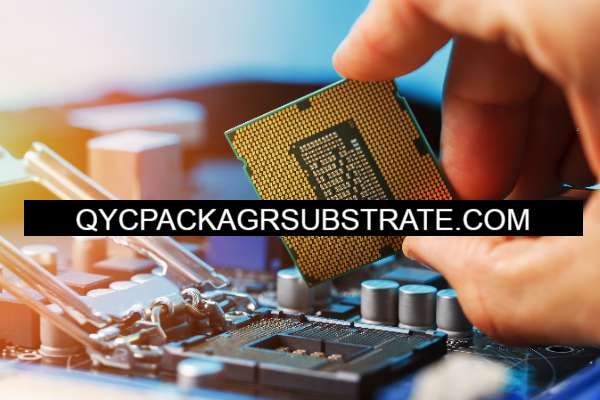
What is an Advanced Glass Substrate (AGS)?
An Advanced Glass Substrate (AGS) is a high-performance substrate material used in the fields of microelectronics and optoelectronics. Compared to traditional silicon, ceramic, and organic substrates, glass substrates offer a range of unique advantages, making them widely applied in high-density packaging, 5G communication, optical devices, and display technologies.
Firstly, glass substrates exhibit excellent electrical properties. Their low dielectric constant and low loss factor contribute to outstanding performance in high-frequency applications, reducing signal transmission losses and delays, thereby enhancing device performance. Additionally, glass substrates have a thermal expansion coefficient close to silicon, effectively reducing thermal stress and improving device reliability and longevity.
Secondly, glass substrates possess superior mechanical properties. They feature high strength, hardness, and good flatness, supporting higher-density integrated circuits and finer line patterns. This makes glass substrates well-suited for the manufacturing of micro and nanoscale devices that require high precision and stability.
Moreover, glass substrates demonstrate excellent chemical stability and environmental adaptability. They resist moisture, chemical agents, and temperature changes, showing high resistance to deformation and corrosion, ensuring long-term stability and reliability.
In terms of manufacturing processes, glass substrate processing technologies continue to advance. Advanced laser processing and etching techniques enable high-precision and high-density microholes and microstructures on glass substrates, meeting the diverse requirements of different application fields.
In conclusion, Advanced Glass Substrates, with their excellent electrical, mechanical, and chemical properties, are becoming crucial materials in the fields of microelectronics and optoelectronics. With ongoing technological advancements and increasing application demands, glass substrates have promising future prospects.
Advanced Glass Substrates Manufacturer
What are the Advanced Glass Substrates Design Guidelines?
The design guidelines for Advanced Glass Substrates (AGS) typically focus on ensuring optimal performance and reliability of electronic and optoelectronic devices fabricated on these substrates. Here are some key aspects covered in AGS design guidelines:
- Electrical Performance: Guidelines ensure that the substrate’s electrical properties, such as dielectric constant, loss tangent, and impedance characteristics, meet the specifications required for the intended application. This includes minimizing signal losses and ensuring signal integrity across high-frequency ranges.
- Mechanical Properties: AGS design guidelines emphasize mechanical stability, including substrate flatness, warpage control, and dimensional accuracy. These properties are critical for supporting precise alignment and assembly processes in device manufacturing.
- Thermal Management: Given the sensitivity of electronic components to heat, AGS design guidelines address thermal properties such as coefficient of thermal expansion (CTE), thermal conductivity, and heat dissipation capabilities. Effective thermal management helps in maintaining device reliability and performance under varying temperature conditions.
- Material Compatibility: Guidelines specify compatibility with different manufacturing processes such as laser processing, etching, and bonding techniques. AGS should exhibit good adhesion properties with metal conductors and dielectric layers used in device fabrication.
- Surface Finish and Coating: Surface finish requirements ensure smoothness and cleanliness suitable for high-resolution patterning and deposition processes. Coating guidelines may include recommendations for anti-reflection coatings, protective layers, or surface treatments to enhance performance and durability.
- Reliability and Durability: AGS design guidelines often incorporate reliability testing criteria, such as thermal cycling, moisture resistance, and mechanical stress tests, to validate substrate performance over its operational lifetime. Ensuring robustness against environmental factors enhances device longevity.
- Design for Manufacturing (DFM): Guidelines may include recommendations for design layouts, via placements, and routing configurations that optimize manufacturing yield and minimize potential defects during fabrication processes.
- Environmental Considerations: Addressing environmental factors like humidity, chemical exposure, and mechanical stress helps in determining the suitable AGS material composition and processing techniques for specific application requirements.
Overall, AGS design guidelines aim to provide comprehensive instructions for designing and manufacturing electronic and optoelectronic devices on glass substrates, ensuring they meet performance, reliability, and cost-efficiency criteria for diverse applications.
What is the Advanced Glass Substrates Fabrication Process?
The fabrication process of Advanced Glass Substrates (AGS) involves several key steps to achieve the desired electrical, mechanical, and thermal properties required for electronic and optoelectronic applications. Here are the general steps involved in the fabrication process of AGS:
- Glass Selection:The process begins with selecting the appropriate type of glass based on the desired electrical characteristics (dielectric constant, loss tangent), mechanical properties (strength, flatness), and thermal properties (thermal expansion coefficient, conductivity).
- Cleaning and Preparation: The selected glass undergoes thorough cleaning to remove contaminants and ensure a clean surface suitable for subsequent processing steps. This step is crucial to achieve proper adhesion and ensure the quality of subsequent layers.
- Laser Processing or Etching: AGS often involves precise patterning of features such as vias, microchannels, or fine line circuits. Laser processing or etching techniques are employed to create these patterns with high accuracy and resolution on the glass substrate. This step is critical for defining the circuitry and interconnections of the electronic devices.
- Dielectric Layer Deposition:Thin dielectric layers (often oxides or nitrides) are deposited onto the glass substrate. These layers serve as insulating barriers between conductive layers, ensuring proper isolation and preventing electrical shorts. Deposition methods can include physical vapor deposition (PVD), chemical vapor deposition (CVD), or other techniques suitable for glass substrates.
- Conductor Deposition: Metal conductors (typically copper or aluminum) are deposited onto the substrate surface or within the defined patterns via processes such as sputtering, evaporation, or electroplating. These conductors form the electrical pathways and interconnects required for the device functionality.
- Surface Finishing: After deposition of conductive and dielectric layers, surface finishing treatments may be applied to enhance surface smoothness, ensure uniformity, and improve adhesion properties for subsequent layers or components.
- Lamination and Bonding: In some cases, multiple layers of AGS may be laminated together using bonding techniques to create multi-layered substrates. This process enhances integration capabilities and allows for complex circuit designs with improved performance.
- Quality Control and Testing: Throughout the fabrication process, quality control measures are implemented to verify dimensional accuracy, material properties, and adherence to design specifications. Testing includes electrical testing, thermal cycling tests, and mechanical stress tests to ensure reliability and functionality of the finished AGS.
- Packaging and Assembly: Once fabricated and tested, AGS substrates are typically packaged and integrated into electronic or optoelectronic devices through assembly processes that may involve soldering, wire bonding, or other connection methods.
The AGS fabrication process combines precision manufacturing techniques with stringent quality control measures to produce substrates that meet the demanding requirements of modern electronic and optoelectronic applications. Each step is critical in ensuring the substrate’s performance, reliability, and suitability for its intended use.
How do you Manufacture an Advanced Glass Substrates?
Manufacturing an Advanced Glass Substrate (AGS) involves a series of specialized steps and processes aimed at producing a high-performance substrate suitable for electronic and optoelectronic applications. Here’s a detailed outline of how AGS is typically manufactured:
- Glass Material Selection: The process begins with selecting a suitable type of glass based on desired electrical, mechanical, and thermal properties. Factors such as dielectric constant, thermal expansion coefficient, strength, and surface flatness are considered.
- Cleaning and Preparation: The selected glass undergoes rigorous cleaning to remove impurities and contaminants. This step is crucial to ensure a clean surface, which is essential for subsequent processing steps and to achieve proper adhesion of deposited layers.
- Laser Processing or Etching: High-precision patterning of features on the glass substrate is achieved using laser processing or etching techniques. This step involves defining microchannels, vias, and circuit traces with exacting accuracy. Laser technology ensures fine resolution and control over the patterned structures.
- Dielectric Layer Deposition: Thin layers of dielectric material, such as oxides or nitrides, are deposited onto the glass substrate. This deposition is typically performed using techniques like physical vapor deposition (PVD) or chemical vapor deposition (CVD). The dielectric layers provide insulation between conductive layers and contribute to the substrate’s electrical performance.
- Conductor Deposition: Metal conductors (commonly copper or aluminum) are deposited onto the substrate surface or within the defined patterns. Deposition methods include sputtering, evaporation, or electroplating, depending on the specific requirements of the design. These conductors form the electrical pathways and interconnects necessary for device functionality.
- Surface Finishing: Surface treatments are applied to ensure smoothness, uniformity, and improved adhesion properties of the substrate. These treatments may involve chemical processes or coatings that enhance the substrate’s surface characteristics and compatibility with subsequent layers.
- Lamination and Bonding (Optional): For advanced applications requiring multi-layered structures, AGS substrates may undergo lamination processes. This involves bonding multiple layers of glass substrates together to create integrated circuits with enhanced performance and functionality.
- Quality Assurance and Testing: Throughout the manufacturing process, stringent quality control measures are implemented to verify dimensional accuracy, material consistency, and adherence to design specifications. Testing includes electrical testing, thermal cycling tests, and mechanical stress tests to ensure the reliability and durability of the AGS substrate.
- Packaging and Integration: Once manufactured and tested, AGS substrates are packaged and integrated into electronic or optoelectronic devices through assembly processes. This final step involves connecting the substrate to other components using techniques such as soldering, wire bonding, or flip-chip bonding.
The manufacturing of AGS requires expertise in glass processing, precision engineering, and materials science to achieve substrates that meet the demanding performance requirements of modern electronic devices. Each step in the manufacturing process contributes to ensuring the substrate’s functionality, reliability, and suitability for its intended application.
How Much Should an Advanced Glass Substrates Cost?
The cost of an Advanced Glass Substrate (AGS) can vary significantly depending on several factors related to its design, materials, manufacturing processes, and specifications. Here are some key factors that influence the cost of AGS:
- Material Selection: The type and quality of glass used for the substrate can impact costs. Glasses with specific properties such as low dielectric constant, high thermal stability, or special surface treatments may be more expensive.
- Complexity of Design: AGS designed with intricate patterns, fine features (microvias, microchannels), or multiple layers will generally cost more due to the increased complexity in manufacturing processes such as laser processing, deposition, and lamination.
- Manufacturing Processes: The choice of manufacturing techniques—such as laser processing, deposition methods (PVD, CVD), and surface treatments—will affect costs. More advanced processes that require specialized equipment and expertise tend to increase manufacturing costs.
- Quality and Reliability Requirements: AGS intended for high-reliability applications, such as aerospace or medical devices, may require additional quality control measures and testing, contributing to higher costs.
- Volume and Scale: Economies of scale play a significant role in determining costs. Larger production volumes typically lower per-unit costs due to optimized manufacturing efficiencies and bulk material purchasing.
- Customization and Special Requirements:AGS tailored to specific customer requirements or with unique features (such as specific thermal expansion coefficients or optical properties) may incur additional customization costs.
- Market Conditions: Market dynamics, including supply chain factors, raw material costs, and competition among suppliers, can influence pricing.
Given these factors, the cost of an AGS can range from a few dollars per square inch to tens or even hundreds of dollars per unit, depending on the complexity and specifications. For precise cost estimates, manufacturers typically provide quotes based on detailed project requirements, including substrate size, thickness, material specifications, and volume orders.
What is Advanced Glass Substrates Base Material?
The base material for an Advanced Glass Substrate (AGS) refers to the primary glass substrate used as the foundation for electronic or optoelectronic devices. AGS base materials are specifically chosen for their electrical, mechanical, thermal, and chemical properties, which are critical for the performance and reliability of the final substrate.
Key characteristics of AGS base materials include:
- Dielectric Constant: AGS base materials typically have a low dielectric constant to minimize signal loss and ensure high-frequency performance in electronic circuits.
- Thermal Stability: They exhibit a stable thermal expansion coefficient to minimize thermal stress and ensure reliability across a range of operating temperatures.
- Mechanical Strength: AGS base materials are engineered to have sufficient mechanical strength and rigidity to support delicate microstructures and withstand assembly processes.
- Surface Quality: The surface of AGS base materials is carefully prepared to be smooth and free of contaminants, facilitating precise patterning and layer deposition during manufacturing.
- Chemical Resistance: They often possess good resistance to chemicals and environmental factors, ensuring long-term stability and reliability in various application environments.
AGS base materials are typically selected based on the specific requirements of the application, such as high-speed data transmission, optical clarity, thermal management, or miniaturization. Different types of glass compositions and formulations may be utilized to achieve these desired properties, with ongoing advancements in glass technology continually expanding the range of available AGS base materials.
Which Company Makes Advanced Glass Substrates?
Currently, several companies manufacture Advanced Glass Substrates (AGS), including AGC Inc. in Japan, Sumitomo Glass, Shin-Etsu Chemical Co., Ltd., and Samsung SDI in Korea. These companies have extensive experience and advanced manufacturing technologies in glass technology, microelectronics, and optoelectronics applications, enabling them to produce AGS products that meet high-performance and high-reliability requirements.
As for our company, if we possess the relevant technology and resources, we can also consider entering the AGS production field. Producing AGS requires mastering advanced glass processing technology, microfabrication techniques, and the application of specialty materials. First, we need to ensure that we have high-precision laser processing equipment and etching equipment suitable for AGS production. These devices can achieve micron-level structural processing and precise pattern definition, meeting the high-density integration needs of electronic and optoelectronic devices.
Secondly, AGS manufacturing involves special requirements for high temperature and chemical resistance. We need to have the capability to select appropriate glass materials and optimize processing techniques to ensure that the substrates maintain stable physical and chemical properties in complex manufacturing environments.
Additionally, AGS manufacturing requires strict quality control and product testing. We need to establish a comprehensive quality management system, including raw material inspection, process monitoring, and thorough testing of the final products. These measures can ensure that every AGS we produce meets the performance requirements and reliability standards of our customers.
In summary, entering the AGS production field not only requires technical strength and production equipment but also an in-depth understanding of market demands and technological trends. If our company meets these conditions and can effectively satisfy customer needs, we will undoubtedly find our place in the advanced glass substrate market and contribute to the industry’s development.
What are the 7 Qualities of Good Customer Service?
The 7 qualities of good customer service are:
- Responsiveness: Promptly addressing customer inquiries, concerns, and requests demonstrates respect for their time and needs.
- Empathy: Understanding and empathizing with the customer’s situation shows genuine care and helps build a positive rapport.
- Clarity: Providing clear and accurate information ensures customers understand their options, solutions, and next steps.
- Patience: Remaining calm and patient, especially during challenging situations, helps de-escalate conflicts and fosters a supportive interaction.
- Effective Communication: Using clear and concise language, active listening, and adjusting communication style to meet the customer’s preferences enhances understanding and satisfaction.
- Problem-solving Skills: Proactively seeking solutions and resolving issues efficiently demonstrates competence and commitment to customer satisfaction.
- Professionalism: Maintaining professionalism through courteous behavior, respect for privacy, and adherence to company policies builds trust and credibility.
These qualities collectively contribute to creating a positive customer experience and fostering long-term customer loyalty.
FAQs
What are Advanced Glass Substrates (AGS)?
AGS are specialized glass materials used as substrates in microelectronics and optoelectronics. They offer high performance in terms of electrical properties, thermal management, and mechanical stability.
What are the advantages of using AGS?
AGS offer advantages such as low dielectric constant, excellent thermal stability, high mechanical strength, and superior surface quality. These properties make them suitable for high-frequency applications, optical devices, and environments requiring reliability and precision.
What applications are AGS used for?
AGS are used in various applications including high-speed data transmission, 5G communication, optical communication systems, display technologies (like OLEDs), and sensors requiring precision and reliability.
How are AGS manufactured?
AGS manufacturing involves processes such as glass material selection, cleaning, precision laser processing or etching for microstructures, deposition of dielectric and conductive layers, surface finishing, quality control, and packaging.
What are the key considerations in choosing AGS?
Factors to consider include electrical properties (dielectric constant, loss tangent), thermal properties (thermal expansion coefficient, conductivity), mechanical strength, surface quality, compatibility with manufacturing processes, and application-specific requirements.
What companies manufacture AGS?
Companies involved in AGS production include AGC Inc., Sumitomo Glass, Shin-Etsu Chemical Co., Ltd., and Samsung SDI, among others, known for their expertise in glass technology and microelectronics.
What are the cost considerations for AGS?
The cost of AGS varies based on factors such as material type, complexity of design, manufacturing processes, quality requirements, and market conditions. Customization and volume orders also influence pricing.