
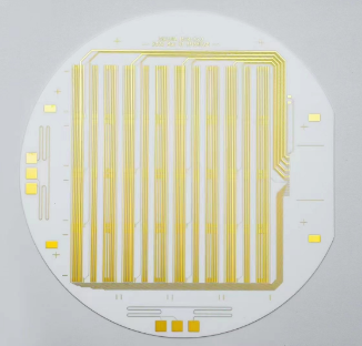
Ceramic ALUMINUM AI2O3 substrate producer. the Package Substrate will be made with ALUMINUM AI2O3 core materials. or other types Ceramic materials. High quality and fast lead time.
A Ceramic Package Substrate assumes a pivotal role in the electronics landscape, tailor-made for the intricacies of semiconductor devices. Forged from ceramic materials like alumina (aluminum oxide) or aluminum nitride, this substrate establishes itself as a sturdy canvas for the assembly and interlinking of a diverse spectrum of electronic components.
Its merits unfold across multiple dimensions:
Exemplary Heat Conductance: Ceramics showcase peerless heat conductivity, deftly diffusing the thermal energy generated by electronic components.
Robust Mechanical Underpinning: Ceramic materials lay down a stable mechanical bedrock, safeguarding the package’s structural soundness and fending off any proclivity for warping or deformation.
Electrical Insulation Proficiency: Doubling as an electrical insulator, ceramics stand as a bulwark against undesirable electrical cross-talk among different components residing on the substrate.
Architect of Miniaturization: With its finesse in manufacturing intricacies, ceramic package substrates empower the art of miniaturizing electronic devices.
Augmented Reliability: The thermal and mechanical prowess of ceramics significantly elevates the overall reliability quotient of electronic components.
These substrates find a sprawling array of applications in packaging integrated circuits (ICs), microprocessors, and the expansive realm of semiconductor devices where adept thermal management and unwavering reliability rank high. They emerge as stalwart guardians, shielding electronic components and streamlining their communion with external circuitry.
What Are the Functions of Ceramic Package Substrate?
In the intricate landscape of electronics, the Ceramic Package Substrate takes center stage, specifically tailored for the intricate dance of semiconductor devices. Let’s unfold the tapestry of its functions:
Anchor of Components: Serving as an unwavering base, the ceramic substrate ensures the secure anchoring of diverse electronic components, spanning the gamut from integrated circuits (ICs) to microprocessors.
Conduit for Connectivity: Operating as a central conduit for connectivity, the substrate orchestrates seamless communication and collaboration among electronic components housed within a packaged unit.
Master of Heat Dissipation: Harnessing the remarkable thermal conductivity of ceramics, the substrate skillfully dissipates the heat generated by electronic components, preempting overheating and ensuring a harmonious performance.
Guardian of Structural Integrity: Contributing to the mechanical resilience of the overall package, ceramic package substrates stand resilient against warping or deformation, preserving the structural integrity of the electronic ensemble.
Electrical Insulation Bastion: The ceramic material stands tall as an electrical insulator, erecting an impervious barrier against unwanted electrical interactions between different components on the substrate.
Pioneer of Miniaturization: With finesse in manufacturing intricacies, ceramic substrates pioneer the art of miniaturization in electronic devices, a transformative force in crafting compact and space-efficient products.
Reliability Virtuoso: The thermal and mechanical finesse of ceramics elevates the overall reliability of electronic components, providing a stable and enduring haven for their continuous operation.
Sentinel of Electronic Kin: Beyond functionality, the substrate metamorphoses into a protective sentinel, shielding enclosed electronic components from potential damage and the vagaries of external environmental factors.
In essence, the Ceramic Package Substrate emerges as a versatile virtuoso, offering a robust platform for mounting, interconnecting, and safeguarding electronic components. Its contributions to thermal regulation and reliability solidify its role as an indomitable force in the realm of electronic devices.
What Are the Different Types of Ceramic Package Substrate?
In the ever-evolving field of electronics, a diverse array of ceramic package substrates is ready to meet a spectrum of needs. Let’s explore the unique attributes of different types:
Alumina (Aluminum Oxide) Substrates:
Overview: Alumina ceramic substrates lead the way, seamlessly merging commendable thermal conductivity with effective electrical insulation.
Applications: Integrated widely into circuits (ICs), microprocessors, and power modules.
Aluminum Nitride (AlN) Substrates:
Overview: Celebrated for outstanding thermal conductivity, aluminum nitride substrates shine in applications demanding efficient heat dissipation.
Applications: Commonly embraced in power electronics, LED packages, and scenarios where robust thermal management is paramount.
Beryllium Oxide (BeO) Substrates:
Overview: Despite remarkable thermal conductivity, the utilization of beryllium oxide substrates has dwindled due to concerns about beryllium’s toxicity.
Applications: Historically prominent in high-performance settings, but diminishing due to health and safety considerations.
Zirconia (ZrO2) Substrates:
Overview: Zirconia ceramic substrates showcase robust mechanical strength and resilience against wear and corrosion.
Applications: Deployed in specific scenarios demanding high mechanical durability, such as sensors and electronics in challenging environments.
Glass Ceramic Substrates:
Overview: Blending ceramic and glass properties, glass ceramic substrates offer a nuanced fusion of thermal and mechanical characteristics.
Applications: Routinely applied in microelectronics, sensors, and contexts requiring a sophisticated interplay of properties.
Silicon Nitride (Si3N4) Substrates:
Overview: Silicon nitride substrates exhibit resilience against thermal shock, addressing applications with elevated temperature demands.
Applications: Engaged in environments requiring resistance to thermal cycling and high temperatures, including automotive sensors and aerospace electronics.
Selecting the optimal ceramic package substrate demands thoughtful consideration of specific characteristics essential for a given electronic device or system. Whether it’s thermal conductivity, electrical insulation, mechanical robustness, or tailored requisites, these substrates unfold as a versatile toolkit, adeptly navigating the dynamic landscape of electronics.
How Does Ceramic Package Substrate Differ from PCB?
Within the intricate tapestry of electronics, ceramic package substrates and printed circuit boards (PCBs) emerge as distinctive players, each weaving a narrative of specialized features and applications. Let’s embark on a journey to unravel the contrasting threads that distinguish ceramic package substrates from PCBs:
Material Symphony:
Ceramic Package Substrates: Crafted from materials such as alumina, aluminum nitride, beryllium oxide, silicon nitride, or glass ceramics, ceramic package substrates conduct a symphony of tailored properties in the realms of electricity, heat, and mechanical resilience.
PCBs: Choreographed from layered sheets of fiberglass-reinforced epoxy resin (FR-4), PCBs dance with versatility, offering a stage for electronic circuits to perform with copper traces and substrate layers.
Architectural Ballet:
Ceramic Package Substrates: Sturdy and monolithic, ceramic package substrates take center stage, providing a steadfast platform meticulously designed for the packaging of semiconductor devices, ensuring a performance of reliability.
PCBs: Executing a ballet of layers, PCBs gracefully laminate substrate, copper traces, and insulating layers, allowing for the choreography of intricate electrical circuits that adapt to diverse electronic compositions.
Electrical Pas de Deux:
Ceramic Package Substrates: With a graceful pirouette, ceramic materials in substrates showcase impeccable electrical insulation properties, earning a standing ovation in applications requiring high-frequency finesse, thermal proficiency, and electrical isolation.
PCBs: Serving as a versatile partner in the dance of electronic connectivity, PCBs provide a stable waltz for components, supporting a wide range of electrical requirements across diverse applications.
Thermal Ballet:
Ceramic Package Substrates: Taking the lead in thermal grace, ceramic substrates perform with heightened thermal conductivity, a virtuoso trait especially valued in applications demanding exquisite heat dissipation, such as in high-power electronic devices.
PCBs: While not the prima ballerina in thermal conductivity, PCBs incorporate features to elegantly dissipate heat, contributing to the overall thermal performance of electronic compositions.
Applications Symphony:
Ceramic Package Substrates: Stepping into the limelight of semiconductor packaging, ceramic package substrates shine in applications where high-frequency precision and robust thermal management take center stage, performing in integrated circuits, microprocessors, and power modules.
PCBs: Taking center stage in the grand electronic symphony, PCBs harmonize with a broad spectrum of devices, from the intricate notes of computers and smartphones to the majestic crescendos of industrial equipment.
In this grand performance of electronics, ceramic package substrates and PCBs waltz and weave, each contributing a unique note to the harmonious composition of electronic systems. The former takes on the role of a specialized soloist in precision packaging, while the latter serves as the versatile ensemble, providing a foundational stage for electronic circuitry across diverse applications.
What Are the Main Structure and Production Technologies of Ceramic Package Substrate?
In the intricate process of crafting ceramic package substrates, a symphony of production technologies orchestrates the creation of a structure that aligns seamlessly with the dynamic needs of the electronic landscape. Let’s explore the ensemble of main structures and production methodologies:
Main Structure:
Ceramic Foundation:
The narrative unfolds with a chosen ceramic material, be it the resilience of alumina, the conductivity of aluminum nitride, the precision of beryllium oxide, the robustness of silicon nitride, or other specialized ceramics.
Layered Tapestry:
Layers intertwine, creating a rich tapestry of functionality. These layers include conductive pathways, insulating layers, and occasionally, specialized functional layers, each playing a distinct role in the substrate’s composition.
Conductive Intricacies:
Artful patterns of conductive traces grace the substrate, forming a network of intricate electrical pathways. Crafted from metals like copper or gold, these traces become the silent performers in the electronic symphony.
Dielectric Harmony:
Harmonious dielectric layers weave through the substrate, providing insulation between conductive traces. The selection of dielectric material is akin to choosing musical notes, ensuring a symphony of electrical and thermal properties.
Metallurgical Flourish:
A metallurgical flourish takes center stage, with the deposition of metal layers. This metallization process adds depth to the substrate, creating bonding pads and defining conductive pathways in a visual and functional masterpiece.
Component Attachment Stages:
Designated areas, adorned with bonding pads and specific metallization, act as stages for the attachment of electronic components. These areas become the platforms where the electronic performance unfolds.
Production Technologies:
Ceramic Prelude:
The journey commences with the preparation of raw ceramic materials, akin to the tuning of instruments before a grand performance. Shaping these materials sets the stage for the substrate’s manufacturing.
Layered Choreography:
Layers gracefully converge through lamination, each layer finding its place in the choreography. The stacking and bonding process, resembling a dance, establish the substrate’s layered structure.
Conductor Ballet:
A conductor ballet ensues, with techniques like photolithography defining the intricate patterns of conductive traces. The substrate undergoes processes, resembling dance steps, to create the desired electrical pathways.
Metallization Overture:
Metallization takes center stage in a grand overture, involving the deposition of metal layers through methods like sputtering or chemical vapor deposition. This step breathes life into the substrate’s conductive pathways and bonding pads.
Dielectric Elegance:
Dielectric layers elegantly settle onto the substrate, their deposition orchestrated through methods like chemical vapor deposition. This adds an element of elegance, ensuring insulation between the electrical pathways.
Etching and Finishing Crescendo:
Excess material gracefully exits the stage through etching processes, and the substrate experiences a finishing crescendo. This finale ensures a polished and uniform surface, ready for the spotlight.
Sintering Symphony:
The grand sintering symphony commences, subjecting the substrate to high temperatures. This transformative process enhances mechanical strength and refines electrical properties, like the crescendo in a musical masterpiece.
Quality Control Sonata:
Throughout this artistic journey, a vigilant quality control sonata plays in the background, ensuring that each substrate meets the high standards and specifications demanded by the electronic composition.
The production of ceramic package substrates unfolds as a symphony of creativity and precision, where each element plays a crucial role in creating a substrate that resonates harmoniously with the intricate demands of electronic applications.
FAQs (Frequently Asked Questions)
What Defines a Ceramic Package Substrate?
A ceramic package substrate is the virtuoso of electronic foundations, a specialized maestro orchestrating stability for electronic components like integrated circuits, microprocessors, and power modules.
Which Symphony of Materials Composes Ceramic Package Substrates?
The ceramic palette includes notes of alumina, aluminum nitride, beryllium oxide, silicon nitride, and glass ceramics, each contributing its unique resonance in the creation of these substrates.
Why Enlist Ceramic Package Substrates for Electronic Performances?
Ceramic package substrates take the stage for their stellar thermal conductivity, electrical insulation prowess, and the robust strength needed for high-performance applications demanding an encore in efficient heat dissipation.
How Does the Artistic Process of Manufacturing Unfold for Ceramic Package Substrates?
The manufacturing masterpiece involves a choreography of substrate preparation, layering through lamination, conductor patterning, metallization, dielectric layer deposition, etching, finishing, sintering, and a finale of quality control to ensure a flawless composition.
In Which Electronic Productions Can Ceramic Package Substrates Steal the Show?
Ceramic package substrates are the stars in semiconductor packaging, gracing the stage in integrated circuits, microprocessors, power modules, and other electronic performances where thermal management takes a bow.
How Can I Request a Melodic Quote for Ceramic Package Substrates?
To summon a harmonious quote, reach out to manufacturers or suppliers, sharing the specifics of your composition – material preferences, dimensions, quantities – to receive a personalized symphony for your electronic production.
What Crescendos Influence the Cost of Ceramic Package Substrates?
The cost composition is orchestrated by the material’s musical choice, the complexity and size of the substrate’s arrangement, the quantity in the ensemble, and any additional notes like specialized coatings that enhance the performance.
Can Ceramic Package Substrates Be Tailored for a Custom Score?
Indeed, many manufacturers offer a customized score for ceramic package substrates. Engage in a creative dialogue with suppliers to articulate your requirements, from material nuances to the dimensions that will resonate with your unique composition.
Are There Overtures of Minimum Order Quantities for Ceramic Package Substrates?
The symphony’s entry ticket may vary among suppliers. It’s advisable to engage in a conversation about minimum order quantities, as this note may change based on the manufacturer’s symphonic arrangements.
What Harmonious Quality Standards Should Echo in Ceramic Package Substrates?
Seek substrates that dance to the rhythm of quality standards, be it the virtuosity of ISO certifications or the adherence to industry standards that ensure these ceramic components perform in perfect harmony within the electronic ensemble.
Conclusion
In conclusion, the realm of ceramic package substrates unfolds as a captivating symphony, where materials, manufacturing processes, and applications harmonize to create a performance worthy of the electronic stage. From the foundational ceramic materials to the intricate choreography of production technologies, each element plays a crucial role in shaping substrates that stand as pillars of strength for electronic components.
The dance of materials, whether it be the resilient alumina, conductive aluminum nitride, or other ceramic virtuosos, showcases a diverse palette that caters to the specific demands of high-performance applications. These substrates, with their exceptional thermal conductivity, electrical insulation, and mechanical resilience, take center stage in semiconductor packaging, contributing to the seamless orchestration of integrated circuits, microprocessors, and power modules.
The manufacturing process, akin to a ballet, involves a series of well-coordinated steps—from substrate preparation to the grand finale of sintering. The conductor’s baton directs layering, conductor patterning, metallization, and dielectric layer deposition, culminating in a masterpiece that undergoes rigorous quality control. This ensures that each substrate meets the stringent standards demanded by the electronic composition.
Requesting a quote for these ceramic performers involves a creative dialogue with manufacturers, where specific material preferences, dimensions, and quantities compose a personalized score. The cost composition is influenced by factors such as material choices, the complexity of the arrangement, size, quantity, and additional embellishments.
Ultimately, ceramic package substrates are not mere components; they are protagonists in the electronic saga, playing a vital role in enabling advanced technologies. As the curtain falls on this exploration, the symphony of ceramic package substrates resonates as a testament to the artistry and precision in the world of electronic packaging.