
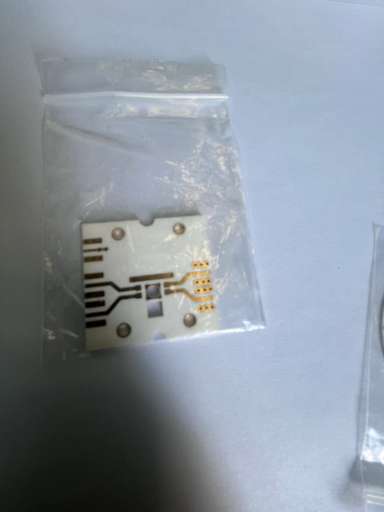
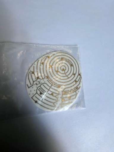
Aluminum Nitride PCB (AlN PCB) Manufacturing
Aluminum Nitride PCB (AlN PCB) Manufacturing, Ceramic ALN PCB and Ceramic 96 AL2O3 PCB Vendor, we offer high quality Ceramic PCBs from 1 layer to 20 layers. we also offer Ceramic package substrates with microtrace and spacing. Aluminum Nitride PCBs, often abbreviated as AlN PCBs, represent a cutting-edge solution in the realm of electronic circuitry. These PCBs utilize Aluminum Nitride, a high-performance ceramic material, as the substrate instead of traditional materials like FR4. Renowned for its exceptional thermal conductivity, electrical insulation, and mechanical strength, Aluminum Nitride offers a myriad of benefits. It efficiently dissipates heat generated by electronic components, ensuring optimal performance even in high-power and high-frequency applications. The superior electrical insulation properties of AlN enable reliable operation, while its robust mechanical strength enhances the durability of the PCB. AlN PCBs find extensive utility in diverse sectors, including telecommunications, aerospace, automotive, and LED lighting. Whether it’s facilitating high-speed data transmission or powering intricate electronic systems, Aluminum Nitride PCBs stand as a testament to innovation, reliability, and performance in modern electronics.
What is an Aluminum Nitride PCB (AlN PCB)?
Aluminum Nitride PCB (AlN PCB) manufacturing.High speed and high frequency material packaging substrate manufacturing. Advanced packaging substrate production process and technology
An Aluminum Nitride PCB (AlN PCB) is a type of printed circuit board (PCB) that utilizes aluminum nitride as the substrate material instead of traditional materials like FR4 (flame retardant 4) or ceramic substrates. Aluminum nitride (AlN) is a ceramic material with excellent thermal conductivity, electrical insulation properties, and high mechanical strength, making it well-suited for use in high-power and high-frequency electronic applications.
AlN PCBs are primarily used in applications where efficient heat dissipation is crucial, such as in high-power RF (radio frequency) amplifiers, power electronics, LED lighting, and high-frequency circuits. The high thermal conductivity of aluminum nitride helps to dissipate heat generated by electronic components more effectively, reducing the risk of overheating and improving overall device performance and reliability.
AlN PCBs can be manufactured using similar processes as traditional PCBs, including etching, plating, and soldering. However, due to the unique properties of aluminum nitride, specialized manufacturing techniques may be required to handle the material properly and ensure good adhesion of circuit traces and components.
Overall, AlN PCBs offer advantages in thermal management, electrical insulation, and mechanical stability, making them suitable for demanding electronic applications where heat dissipation is a critical concern.
What are the Aluminum Nitride PCB Design Guidelines?
Designing with Aluminum Nitride (AlN) PCBs requires careful consideration of the material properties and specific manufacturing processes. Here are some general design guidelines for Aluminum Nitride PCBs:
- Thermal Considerations: AlN PCBs are chosen for their excellent thermal conductivity. Ensure that the heat generated by components can efficiently dissipate through the AlN substrate. Place high-power components strategically to minimize thermal hotspots.
- Material Thickness: AlN PCBs typically come in various thicknesses. Choose the appropriate thickness based on thermal requirements and mechanical constraints. Thicker substrates offer better mechanical stability but may have slower heat dissipation.
- Copper Traces and Planes: Design copper traces and planes carefully to minimize thermal barriers. Use wider traces for higher current-carrying capability and better thermal conductivity.
- Component Placement: Consider the placement of components to optimize heat dissipation and signal integrity. Group high-power components together and keep them away from sensitive signal traces.
- Via Placement: Use vias effectively for thermal management. Place vias strategically to connect copper planes for efficient heat transfer away from critical components.
- Solder Mask: Apply solder mask carefully, especially over high-power components, to prevent short circuits while ensuring good thermal contact with the AlN substrate.
- Soldering Process: Due to the high thermal conductivity of AlN, special soldering techniques may be required. Ensure compatibility with assembly processes such as reflow soldering or wave soldering.
- Electrical Isolation: Although AlN is a good electrical insulator, ensure proper electrical isolation between conductive traces and components to prevent short circuits.
- Mechanical Considerations: AlN PCBs offer good mechanical strength, but avoid placing excessive stress on the substrate during assembly or operation to prevent cracking.
- Environmental Considerations: Consider the operating environment of the PCB, including temperature fluctuations and humidity, and design accordingly to maintain reliable performance over the product’s lifetime.
- Manufacturability: Work closely with the PCB manufacturer to ensure that the design is manufacturable with AlN substrate materials. Consider any specific manufacturing constraints or requirements.
By following these guidelines, designers can optimize the performance, reliability, and manufacturability of Aluminum Nitride PCBs for various high-power and high-frequency electronic applications.
Aluminum Nitride PCB (AlN PCB)
What is the Aluminum Nitride PCB Fabrication Process?
The fabrication process for Aluminum Nitride (AlN) PCBs involves several steps, similar to traditional PCB manufacturing processes, but with considerations for handling the unique properties of AlN substrate material. Here’s a general outline of the fabrication process:
- Substrate Preparation:
– Start with a clean sheet of Aluminum Nitride substrate material in the desired thickness.
– The substrate may come in various sizes and thicknesses depending on the specific application requirements.
- Surface Preparation:
– Clean the surface of the Aluminum Nitride substrate thoroughly to remove any contaminants or residues that could affect adhesion or solderability.
- Circuit Design:
– Design the circuit layout using PCB design software, considering the specific requirements of the application, component placement, signal integrity, and thermal management.
- Photoresist Application:
– Apply a layer of photoresist material onto the surface of the Aluminum Nitride substrate.
– The photoresist will be used to transfer the circuit pattern onto the substrate during the etching process.
- Exposure and Development:
– Expose the photoresist layer to UV light through a photomask containing the circuit pattern.
– Develop the exposed photoresist to remove the unexposed areas, leaving behind the desired circuit pattern on the substrate surface.
- Etching:
– Use chemical etchants to remove the exposed areas of the Aluminum Nitride substrate not protected by the developed photoresist.
– Etching creates the circuit traces and features according to the design pattern.
- Copper Deposition:
– Deposit a thin layer of copper onto the exposed areas of the substrate, forming the conductive traces and pads.
– Copper deposition can be achieved through processes such as electroplating or sputtering.
- Solder Mask Application:
– Apply a solder mask layer over the entire surface of the substrate, leaving openings for component pads and vias.
– The solder mask helps protect the copper traces, provides insulation, and defines the solderable areas for component attachment.
- Silkscreen Printing (Optional):
– Optionally, apply silkscreen printing for labeling component designators, logos, or other identifying information on the PCB surface.
- Surface Finish:
– Apply a surface finish to the exposed copper pads to enhance solderability and prevent oxidation.
– Common surface finishes for AlN PCBs include immersion silver, immersion gold, or OSP (organic solderability preservative).
- Component Assembly:
– Mount electronic components onto the PCB using soldering techniques appropriate for Aluminum Nitride substrate material, such as reflow soldering or wave soldering.
- Testing and Inspection:
– Conduct electrical testing and visual inspection to ensure the integrity and functionality of the fabricated Aluminum Nitride PCB.
- Final Finishing:
– Trim excess material and perform final cleaning and inspection before packaging the finished PCB for shipment.
Throughout the fabrication process, it’s important to adhere to specific handling and processing guidelines for Aluminum Nitride material to prevent damage or contamination that could affect the performance and reliability of the final PCB product. Additionally, collaboration with experienced PCB manufacturers familiar with AlN substrate materials can ensure successful fabrication and optimal performance of AlN PCBs.
Ceramic PCB
How do you manufacture an Aluminum Nitride PCB?
Manufacturing an Aluminum Nitride (AlN) PCB involves a series of steps that are similar to traditional PCB manufacturing processes, with some specific considerations due to the unique properties of AlN substrate material. Here’s a step-by-step guide to manufacturing an AlN PCB:
- Substrate Selection: Choose Aluminum Nitride substrate material of the desired thickness and size according to the specific requirements of the application.
- Surface Preparation: Clean the surface of the Aluminum Nitride substrate thoroughly to remove any contaminants or residues that could affect adhesion or solderability.
- Circuit Design: Design the circuit layout using PCB design software, considering factors such as component placement, signal integrity, thermal management, and electrical insulation.
- Transfer Circuit Pattern: Use a photolithography process to transfer the designed circuit pattern onto the Aluminum Nitride substrate. This involves applying a layer of photoresist, exposing it to UV light through a photomask, and developing it to create the circuit pattern.
- Etching: Use chemical etchants to remove the exposed areas of the Aluminum Nitride substrate not protected by the developed photoresist. This creates the circuit traces and features according to the design pattern.
- Copper Deposition: Deposit a thin layer of copper onto the exposed areas of the substrate, forming the conductive traces and pads. Copper deposition can be achieved through processes such as electroplating or sputtering.
- Solder Mask Application: Apply a solder mask layer over the entire surface of the substrate, leaving openings for component pads and vias. The solder mask protects the copper traces, provides insulation, and defines the solderable areas for component attachment.
- Silkscreen Printing (Optional): Apply silkscreen printing for labeling component designators, logos, or other identifying information on the PCB surface.
- Surface Finish: Apply a surface finish to the exposed copper pads to enhance solderability and prevent oxidation. Common surface finishes for AlN PCBs include immersion silver, immersion gold, or OSP (organic solderability preservative).
- Component Assembly: Mount electronic components onto the PCB using soldering techniques appropriate for Aluminum Nitride substrate material, such as reflow soldering or wave soldering.
- Testing and Inspection: Conduct electrical testing and visual inspection to ensure the integrity and functionality of the fabricated Aluminum Nitride PCB.
- Final Finishing: Trim excess material and perform final cleaning and inspection before packaging the finished PCB for shipment.
Throughout the manufacturing process, it’s essential to adhere to specific handling and processing guidelines for Aluminum Nitride material to prevent damage or contamination that could affect the performance and reliability of the final PCB product. Collaboration with experienced PCB manufacturers familiar with AlN substrate materials can ensure successful fabrication and optimal performance of AlN PCBs.
How much should an Aluminum Nitride PCB cost?
The cost of an Aluminum Nitride (AlN) PCB can vary significantly depending on various factors such as size, complexity, substrate thickness, copper layer thickness, surface finish, quantity, and the specific requirements of the application. Here are some factors that can influence the cost:
- Substrate Material: Aluminum Nitride material tends to be more expensive than traditional PCB substrate materials like FR4. The cost of the AlN substrate will depend on factors such as purity, quality, and thickness.
- Manufacturing Processes: Certain manufacturing processes, such as photolithography and chemical etching, may require specialized equipment and expertise, which can add to the overall cost.
- Copper Thickness: Thicker copper layers generally increase the cost of PCB fabrication due to the additional material and processing required.
- Surface Finish: The choice of surface finish, such as immersion silver, immersion gold, or OSP, can affect the cost of the PCB. Some surface finishes may be more expensive than others.
- Complexity: The complexity of the PCB design, including the number of layers, the density of components, and the intricacy of the circuitry, can impact manufacturing costs.
- Quantity: Typically, larger production runs result in lower per-unit costs due to economies of scale. Ordering larger quantities of AlN PCBs may reduce the cost per board.
- Lead Time: Expedited production or shorter lead times may incur additional costs.
Given these factors, it’s challenging to provide a specific cost without knowing the details of the PCB design and the manufacturing requirements. Generally, AlN PCBs are more expensive than traditional PCBs due to the cost of the substrate material and the specialized manufacturing processes involved.
For a precise cost estimate, it’s advisable to consult with PCB manufacturers who specialize in Aluminum Nitride substrates. They can review the PCB design specifications and provide a quotation based on the specific requirements of the project.
What is Aluminum Nitride PCB base material?
The base material of an Aluminum Nitride (AlN) PCB is Aluminum Nitride itself. Aluminum Nitride is a ceramic compound composed of aluminum and nitrogen atoms. It has excellent thermal conductivity, high electrical insulation properties, and good mechanical strength, making it an ideal material for high-power and high-frequency electronic applications where efficient heat dissipation is crucial.
Aluminum Nitride PCBs are manufactured using Aluminum Nitride ceramic substrates as the foundation. These substrates come in various sizes, thicknesses, and configurations to accommodate different PCB designs and applications. During the fabrication process, circuit patterns are typically etched onto the surface of the Aluminum Nitride substrate, and conductive traces are deposited to create the electrical pathways for components.
Overall, Aluminum Nitride serves as both the structural support and the insulating material for the PCB, providing the necessary thermal and electrical properties required for reliable performance in demanding electronic applications.
Which company makes Aluminum Nitride PCBs?
There are many companies currently producing Aluminum Nitride (AlN) PCBs in the market, some of the well-known manufacturers include Rogers Corporation from the United States, Kyocera from Japan, and CoorsTek from Japan as well. These companies possess advanced technology and equipment, focusing on producing high-quality AlN PCBs to meet various demands in high-power and high-frequency electronic applications.
As for our company, we are a professional electronic manufacturing service provider with abundant experience and a professional team capable of producing Aluminum Nitride (AlN) PCBs. We are committed to providing high-quality PCB solutions tailored to meet specific customer requirements and application needs. Here are the key advantages and capabilities of our company in producing AlN PCBs:
- Professional Team: We have experienced engineers and technicians with profound knowledge and expertise in electronic manufacturing. They can provide customized AlN PCB solutions according to customer design requirements and application scenarios.
- Advanced Equipment: We are equipped with advanced production equipment and process technology to efficiently and precisely manufacture AlN PCBs. Our equipment can meet the processing needs of complex circuit boards, ensuring product quality and stability.
- Strict Quality Control: We strictly adhere to international standards and industry regulations, implementing comprehensive quality control systems from raw material procurement to production processing, and final product inspection. Every step is conducted according to high-quality standards.
- Flexible Production Capacity: We have flexible production capabilities to meet various specifications, sizes, and quantities of orders. Whether it’s small-scale customization or large-scale production, we can meet customer requirements and ensure timely delivery.
- Customer Service: We value communication and cooperation with customers, always prioritizing customer satisfaction. We provide comprehensive customer service support, including technical consultation, sample production, order tracking, etc., ensuring customers receive timely support and assistance throughout the collaboration process.
In conclusion, our company has the technical capabilities and production capacity to produce Aluminum Nitride (AlN) PCBs, and we are dedicated to providing high-quality, customized solutions for our customers. We are committed to offering quality products and services, working together with customers to achieve mutual success.
What are the 7 qualities of good customer service?
Good customer service is characterized by several key qualities that contribute to positive interactions and relationships between businesses and their customers. Here are seven qualities of good customer service:
- Responsiveness: A good customer service team responds promptly to customer inquiries, questions, and concerns. This includes acknowledging messages or calls in a timely manner and providing timely resolutions to issues.
- Empathy: Empathy involves understanding and relating to the customer’s feelings, concerns, and perspectives. Good customer service representatives demonstrate empathy by actively listening to customers, acknowledging their emotions, and showing genuine concern for their needs.
- Professionalism: Professionalism is essential in all customer interactions. It involves maintaining a courteous and respectful demeanor, using proper language and tone, and adhering to company policies and standards.
- Knowledgeability: Good customer service representatives possess thorough knowledge about the products or services offered by the company. They can provide accurate information, answer questions, and offer relevant recommendations to help customers make informed decisions.
- Efficiency: Efficient customer service involves resolving issues or fulfilling requests quickly and effectively. This includes streamlining processes, minimizing wait times, and finding solutions that meet the customer’s needs without unnecessary delays.
- Flexibility: Flexibility is important in adapting to the diverse needs and preferences of customers. Good customer service teams are adaptable and can tailor their approach to accommodate different situations, preferences, and communication styles.
- Consistency: Consistency in customer service ensures that customers receive the same level of quality and support across all interactions and touchpoints with the company. This includes maintaining consistent communication channels, service standards, and problem-solving approaches.
By embodying these qualities, businesses can foster positive customer experiences, build trust and loyalty, and establish strong, long-lasting relationships with their customers.
FAQs
What are the advantages of Aluminum Nitride PCBs?
Aluminum Nitride PCBs offer excellent thermal conductivity, electrical insulation, and mechanical stability, making them ideal for high-power and high-frequency applications.
Can Aluminum Nitride PCBs be used for LED lighting?
Yes, Aluminum Nitride PCBs are commonly used in LED lighting applications due to their efficient heat dissipation properties.
Is Aluminum Nitride PCB fabrication different from traditional PCB fabrication?
Yes, Aluminum Nitride PCB fabrication involves specialized processes to handle the unique properties of the ceramic substrate material.
What is the typical lead time for Aluminum Nitride PCB manufacturing?
Lead times for Aluminum Nitride PCBs can vary depending on factors such as design complexity and production volume, but they typically range from several days to a few weeks.