Cavity PCB
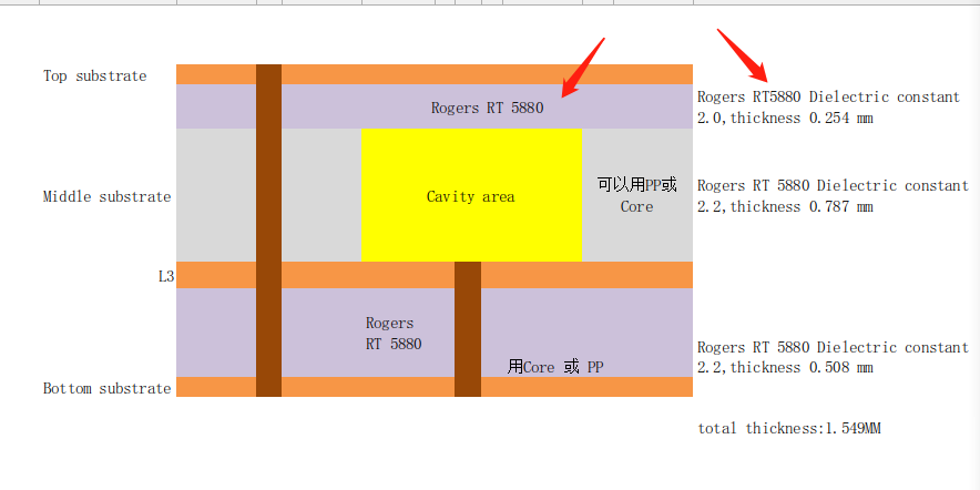
Cavity PCB Manufacturer, Open cavity on the PCBs. Control the depth of the Cavity and the size of the gap. We specialize in producing this kind of Cavity PCBs. To use the Rogers materials, or other types PCB materials.
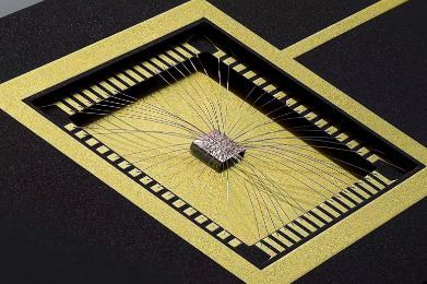
Cavity PCBs, also known as cavity boards or cavity-based printed circuit boards, are specialized PCBs that feature recessed areas within the board itself. These recessed areas, or cavities, are milled or routed into the substrate, creating pockets where components can be mounted flush with the board surface or housed for various purposes.
Cavity PCBs are commonly used in applications where space is at a premium, and component height needs to be minimized. They offer several advantages, including improved thermal management, reduced overall profile, and enhanced protection for sensitive components. Additionally, cavity PCBs can help mitigate electromagnetic interference (EMI) by providing shielding effects.
These PCBs find applications in diverse industries such as aerospace, automotive, medical devices, telecommunications, and consumer electronics. With careful design and manufacturing, cavity PCBs can optimize space utilization, enhance performance, and contribute to the development of compact and efficient electronic systems.
What is a Cavity PCB?
A “Cavity PCB” refers to a type of printed circuit board (PCB) design that includes one or more recessed areas, or cavities, within the board itself. These recessed areas are typically created by milling or routing out portions of the PCB substrate, leaving behind raised areas or walls that define the boundaries of the cavities.
Cavity PCBs are often used in applications where components need to be mounted flush with the surface of the board or where space constraints are particularly tight. By recessing components into cavities within the PCB, it’s possible to reduce the overall profile of the assembled electronics, making them more compact and potentially allowing for integration into smaller devices.
Cavity PCBs are commonly used in industries such as aerospace, automotive, medical devices, and consumer electronics, where miniaturization and space optimization are critical design considerations. They offer advantages such as improved thermal management, protection for sensitive components, and reduced electromagnetic interference (EMI) due to shielding effects provided by the PCB substrate.
Overall, the use of cavity PCBs can help designers achieve more efficient and compact electronic systems while maintaining high levels of performance and reliability.

Buried Cavity PCB
What are Cavity PCB Design Guidelines?
Here are some general guidelines for designing cavity PCBs:
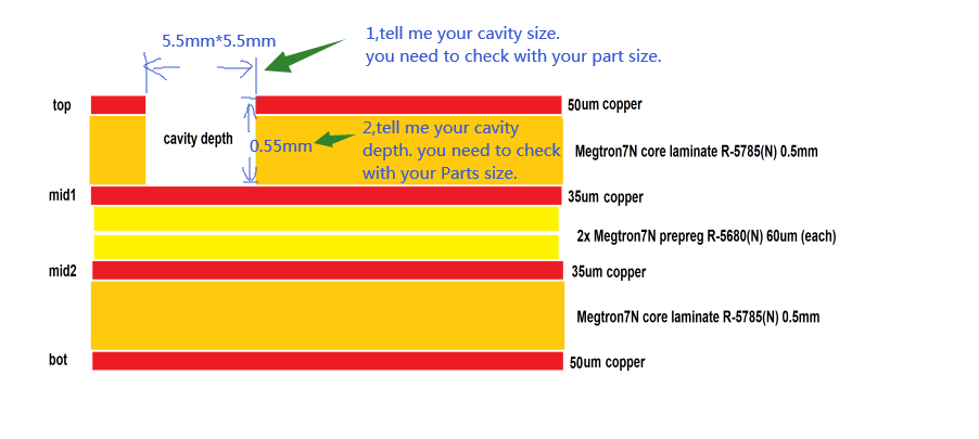
- Define Cavity Dimensions: Clearly define the dimensions of the cavities, including width, length, and depth, based on the components to be housed within them and any space constraints.
- Consider Material Selection: Choose PCB materials that are suitable for cavity designs, such as materials with good milling or routing properties. Ensure that the selected materials offer sufficient mechanical strength and thermal properties.
- Component Placement: Plan component placement carefully to ensure that components fit within the cavities without interference. Consider the height and orientation of components to optimize space utilization.
- Thermal Management: Incorporate thermal management strategies, such as heat sinks or thermal vias, to dissipate heat generated by components within the cavities effectively.
- Signal Integrity: Pay attention to signal integrity considerations, especially for high-speed circuits. Minimize signal distortion and EMI by carefully routing signal traces and providing adequate shielding.
- Mechanical Stability: Ensure that the PCB remains mechanically stable despite the presence of cavities. Reinforce the board structure as needed to prevent warping or flexing.
- EMI Shielding: Utilize the PCB substrate as a natural shield for components housed within cavities. Additionally, consider adding additional shielding layers or coatings if necessary to further reduce electromagnetic interference.
- Manufacturability: Design the PCB with manufacturability in mind. Consider the capabilities of PCB fabrication and assembly processes, such as milling, routing, and component placement.
- Documentation: Provide detailed documentation of cavity dimensions, component placement, and any special requirements to ensure accurate fabrication and assembly of the PCB.
- Testing and Validation: Conduct thorough testing and validation of the cavity PCB design to ensure functionality, reliability, and compliance with specifications.
By following these guidelines, designers can create cavity PCBs that meet the requirements of their specific applications while maximizing performance, reliability, and manufacturability.

Step Cavity PCB
What is the Cavity PCB Fabrication Process?
The fabrication process for cavity PCBs involves several key steps, which are similar to those for standard PCBs but with additional considerations for creating the cavities. Here’s an overview of the cavity PCB fabrication process:
- Design Phase: The process begins with the design of the PCB layout, including the placement of components and the definition of cavity dimensions. CAD software is typically used for this purpose, allowing designers to create detailed layouts and specifications.
- Material Selection: Choose PCB materials suitable for cavity designs, considering factors such as mechanical strength, thermal properties, and compatibility with milling or routing processes.
- Substrate Preparation: Prepare the PCB substrate by laminating layers of copper-clad laminate material. The number of layers and their thicknesses depend on the specific design requirements.
- Drilling and Plating: Drill holes for vias and through-holes as needed for component mounting and interconnection. After drilling, the holes are plated with conductive material to establish electrical connections between layers.
- Cavity Milling or Routing: Use milling or routing machines to create the cavities within the PCB substrate. The cavities are typically milled or routed to the specified dimensions, leaving behind raised areas or walls that define the boundaries of the cavities.
- Copper Plating and Etching: Apply a layer of copper over the entire surface of the PCB, including the walls of the cavities, using electroplating techniques. Then, selectively etch away excess copper to define the circuit traces and copper features.
- Lamination and Pressing: If the PCB design includes multiple layers, laminate the individual layers together using heat and pressure to bond them into a single, multilayered PCB.
- Component Assembly: Mount components onto the PCB surface or within the cavities using soldering or other attachment methods. Pay attention to component placement to ensure they fit properly within the cavities without interference.
- Testing and Inspection: Perform electrical testing and visual inspection to verify the functionality and quality of the fabricated PCB. This may include continuity testing, impedance testing, and inspection for defects or irregularities.
- Finishing: Apply any necessary surface finishes, such as solder mask and silkscreen, to protect the PCB and provide labeling for components and traces.
- Quality Assurance: Conduct final quality checks to ensure that the fabricated cavity PCB meets all design specifications and standards.
Throughout the fabrication process, attention to detail and adherence to design specifications are crucial to ensure the successful creation of cavity PCBs that meet the requirements of their intended applications.

Top side cavity PCBs
How do you manufacture a Cavity PCB?
Manufacturing a cavity PCB involves several steps, including designing the PCB, preparing the substrate, creating the cavities, and assembling components. Here’s a general overview of the process:
- Designing the PCB: Utilize PCB design software to create a layout that includes the desired cavities, component placements, and routing of traces. Ensure that the design meets the electrical and mechanical requirements of the application.
- Selecting Materials: Choose suitable PCB materials that can withstand the milling or routing process required for creating cavities. Consider factors such as substrate thickness, dielectric properties, and thermal conductivity.
- Preparing the Substrate: Start with a blank PCB substrate, typically made of fiberglass-reinforced epoxy resin. Clean the substrate surface to remove any contaminants that could affect the manufacturing process.
- Creating Cavities: Use precision milling or routing equipment to carve out the cavities according to the design specifications. This process requires careful control of depth, width, and dimensions to ensure accuracy.
- Surface Treatment: Apply surface treatments such as copper plating or solder mask to protect the exposed areas of the PCB substrate and facilitate soldering of components.
- Component Assembly: Place and solder the electronic components onto the PCB according to the design layout. Ensure that components fit securely within the cavities and make proper electrical connections.
- Quality Control: Conduct thorough inspection and testing of the completed PCBs to verify functionality, electrical continuity, and mechanical integrity. Use techniques such as automated optical inspection (AOI) and functional testing to identify any defects.
- Finishing Processes: Complete any necessary finishing processes, such as applying conformal coating or silk-screening labels, to enhance durability and readability of the PCB.
- Packaging and Shipping: Package the finished PCBs securely for protection during shipping and handling. Ensure that appropriate documentation accompanies the PCBs for traceability and quality assurance purposes.
Throughout the manufacturing process, it’s essential to maintain strict quality control measures to ensure that the final cavity PCBs meet the required specifications for performance, reliability, and functionality. Collaboration between PCB designers, fabricators, and assemblers is crucial to achieve successful manufacturing outcomes.
How much should a Cavity PCB cost?
The cost of manufacturing a cavity PCB can vary significantly depending on several factors:
- Board Size and Complexity: Larger and more complex cavity PCBs typically require more materials and labor, resulting in higher costs.
- Material Selection: The choice of PCB substrate material can influence the cost. High-performance materials may be more expensive than standard FR-4, but they might offer benefits such as better thermal conductivity or reduced signal loss.
- Cavity Depth and Dimensions: Deeper or larger cavities may require specialized manufacturing processes, such as controlled-depth milling or laser cutting, which can add to the overall cost.
- Layer Count: The number of layers in the PCB affects the fabrication complexity and thus the cost. Cavity PCBs with multiple layers may be more expensive to manufacture.
- Surface Finish and Coating: Different surface finishes and coatings can impact the cost. For example, ENIG (Electroless Nickel Immersion Gold) is a common surface finish but can be more expensive than HASL (Hot Air Solder Leveling).
- Quantity: The volume of PCBs ordered can affect the per-unit cost. Higher quantities often lead to volume discounts from manufacturers.
- Additional Processes: Any additional processes required, such as impedance control, blind/buried vias, or special testing, will add to the cost.
- Supplier: Different PCB manufacturers may offer different pricing structures, so it’s essential to obtain quotes from multiple suppliers to compare costs.
To get an accurate estimate of the cost of manufacturing a cavity PCB, it’s recommended to contact PCB manufacturers and provide them with detailed specifications of your design for a quotation.
What is Cavity PCB base material?
The choice of base material for a cavity PCB depends on various factors such as the application requirements, thermal considerations, mechanical strength, and manufacturing processes involved. However, commonly used base materials for cavity PCBs include:
- FR-4 (Fire Retardant 4): FR-4 is a widely used and cost-effective substrate material for PCBs. It consists of a woven fiberglass cloth impregnated with an epoxy resin binder. FR-4 offers good electrical insulation properties, mechanical strength, and is suitable for standard milling or routing processes to create cavities.
- High-Temperature FR-4: For applications where elevated temperatures are expected, high-temperature FR-4 variants may be used. These materials offer improved thermal stability and can withstand higher operating temperatures without compromising performance.
- Rogers or Teflon-Based Materials: In applications requiring high-frequency performance or strict signal integrity requirements, specialty materials such as Rogers laminates or Teflon-based substrates may be preferred. These materials offer low dielectric loss and excellent electrical properties, making them suitable for cavity PCBs used in RF and microwave applications.
- Metal Core PCBs: For applications requiring enhanced thermal conductivity or heat dissipation, metal core PCBs may be used as the base material. These PCBs typically feature a metal core (such as aluminum or copper) sandwiched between layers of dielectric material. Metal core PCBs are commonly used in LED lighting, power electronics, and automotive applications.
- Ceramic Substrates: In certain high-power or high-frequency applications, ceramic substrates may be utilized due to their excellent thermal conductivity, high dielectric strength, and stability over a wide temperature range.
The selection of the base material should be based on a thorough evaluation of the specific requirements and constraints of the application, considering factors such as electrical performance, thermal management, mechanical properties, and cost.
Which company makes Cavity PCBs?
There are many companies that produce cavity PCBs, including well-known PCB manufacturers and suppliers both domestically and internationally. These companies typically possess advanced manufacturing equipment, extensive experience, and professional teams to meet the needs of various industries.
As a PCB manufacturing company with rich experience and advanced technology, we also have the capability to produce high-quality cavity PCBs. Equipped with advanced processing equipment, including precision CNC milling machines and cutting devices, we can accurately fabricate cavities of various shapes and sizes. Moreover, our team comprises experienced engineers and technicians who can provide customized solutions to clients while ensuring product quality and delivery schedules.
Our cavity PCB manufacturing process strictly adheres to industry standards and quality management systems, ensuring stable and reliable product performance. We also offer comprehensive customer service and support, including technical consultation, sample production, production tracking, and after-sales service, to meet various customer needs.
Whether in aerospace, automotive, medical devices, or consumer electronics industries, we can provide customers with high-quality cavity PCB products and collaborate with them to successfully implement projects. We are committed to providing customers with high-quality products and services, becoming their trusted partners.
What are the 7 qualities of good customer service?
Good customer service is characterized by several key qualities that contribute to positive interactions between a company and its customers. Here are seven qualities of good customer service:
- Responsiveness: A good customer service team responds promptly to customer inquiries, concerns, and requests. They acknowledge customer communications quickly and work efficiently to provide solutions or assistance.
- Empathy: Empathy is crucial in understanding and relating to customers’ feelings, frustrations, and needs. Good customer service representatives show genuine empathy towards customers, demonstrating that they understand their concerns and are committed to helping resolve them.
- Professionalism: Professionalism encompasses aspects such as politeness, respectfulness, and maintaining a positive attitude. Customer service representatives should conduct themselves professionally at all times, regardless of the nature of the customer interaction.
- Knowledgeability: A good customer service team is knowledgeable about the products or services offered by the company. Representatives should be well-trained and equipped with the necessary information to address customer inquiries accurately and effectively.
- Problem-solving skills: Effective problem-solving skills are essential for resolving customer issues and concerns efficiently. Customer service representatives should be resourceful, proactive, and capable of finding creative solutions to meet customers’ needs.
- Consistency: Consistency in service delivery is key to building trust and reliability with customers. Good customer service should be consistent across all channels and interactions, ensuring that customers receive the same high level of service every time.
- Follow-up: Following up with customers after resolving an issue or fulfilling a request demonstrates commitment and concern for their satisfaction. Good customer service teams follow up with customers to ensure that their needs have been met and to gather feedback for continuous improvement.
By embodying these qualities, companies can cultivate strong customer relationships, foster loyalty, and differentiate themselves in the marketplace.
FAQs (Frequently Asked Questions)
What are Cavity PCBs used for?
Cavity PCBs are commonly used in electronic devices and systems where space optimization and component integration are critical. They are often employed in industries such as aerospace, telecommunications, medical devices, and automotive electronics.
Can Cavity PCBs be manufactured in different shapes and sizes?
Yes, Cavity PCBs can be manufactured in various shapes and sizes to accommodate specific design requirements. Custom shapes and dimensions can be achieved using advanced machining and fabrication techniques.
Are Cavity PCBs more expensive than standard PCBs?
Generally, Cavity PCBs may incur slightly higher manufacturing costs due to the additional processes involved in creating cavities and ensuring dimensional accuracy. However, the overall cost depends on factors such as complexity, volume, and material selection.
What are the advantages of using Cavity PCBs?
Some advantages of Cavity PCBs include reduced overall size and weight of electronic assemblies, improved thermal management, enhanced electromagnetic shielding, and increased design flexibility for densely populated circuits.
Can Cavity PCBs be used for high-frequency applications?
Yes, Cavity PCBs can be designed and manufactured to meet the requirements of high-frequency applications, such as RF (radio frequency) and microwave circuits. Specialized materials and design considerations are employed to optimize signal integrity and minimize signal loss.
 Flip-Chip Package Substrate manufacturer
