
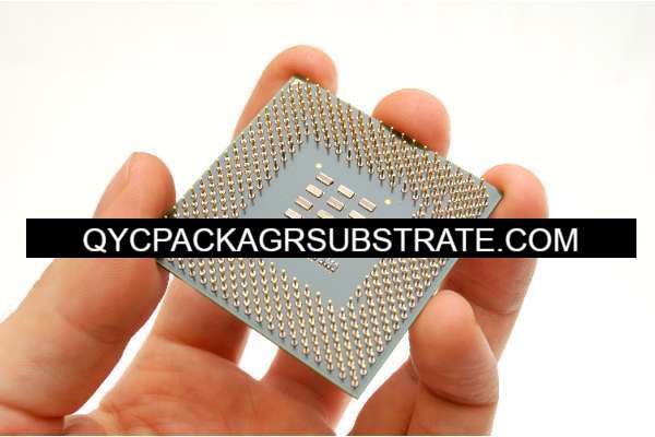
What is Ceramic package substrate?
Ceramic package substrate Manufacturer.High speed and high frequency material packaging substrate manufacturing. Advanced packaging substrate production process and technology.
A ceramic package substrate, also known as a ceramic substrate or ceramic interposer, is a type of packaging technology used in integrated circuits (ICs) and microelectronic devices. It serves as a platform for mounting and interconnecting various electronic components within a semiconductor device.
Ceramic substrates are made from ceramic materials such as alumina (Al2O3) or aluminum nitride (AlN). These materials offer several advantages over traditional organic substrates like printed circuit boards (PCBs), including:
Thermal conductivity: Ceramic substrates have higher thermal conductivity compared to organic substrates, allowing for efficient dissipation of heat generated by the integrated circuits.
Electrical insulation: Ceramic materials have excellent electrical insulation properties, which help prevent leakage currents and ensure proper isolation between different components on the substrate.
Mechanical strength: Ceramic substrates exhibit high mechanical strength and rigidity, providing better reliability and durability compared to organic substrates.
Dimensional stability: Ceramic materials have low coefficients of thermal expansion, meaning they maintain their shape and dimensions even when subjected to temperature variations, ensuring precise alignment of components.
Ceramic package substrates are commonly used in high-performance applications such as microprocessors, graphics processors, memory modules, and high-frequency communication devices where thermal management, electrical performance, and reliability are critical requirements.
Ceramic package substrate Manufacturer
What are the Functions of Ceramic package substrate?
Ceramic package substrates serve several important functions in integrated circuits (ICs) and microelectronic devices. Some of the key functions include:
Mounting surface: Ceramic substrates provide a stable and robust mounting surface for attaching integrated circuit chips, passive components, and other electronic devices. The flat and rigid nature of ceramic substrates ensures precise alignment and secure attachment of components.
Interconnection: Ceramic substrates facilitate the interconnection of various electronic components through metal traces, vias, and bonding pads. These interconnections enable the flow of electrical signals between different parts of the integrated circuit, ensuring proper functionality.
Electrical insulation: Ceramic materials used in package substrates possess excellent electrical insulation properties, preventing unintended electrical connections and leakage currents between adjacent components. This insulation is crucial for maintaining signal integrity and preventing malfunctions or damage due to electrical interference.
Thermal management: Ceramic substrates have high thermal conductivity, allowing them to efficiently dissipate heat generated by the integrated circuit chips. By providing a pathway for heat to escape from the semiconductor devices, ceramic substrates help prevent overheating and ensure the reliable operation of the electronic system.
Mechanical support: Ceramic package substrates offer mechanical support and protection to the delicate semiconductor chips and other electronic components mounted on them. The rigid structure of ceramic materials helps minimize the risk of mechanical damage, such as bending or cracking, during handling, assembly, and operation of the electronic device.
Dimensional stability: Ceramic substrates exhibit low coefficients of thermal expansion, meaning they maintain their shape and dimensions even when exposed to temperature variations. This dimensional stability is essential for ensuring the long-term reliability and performance of the integrated circuit package, particularly in applications with wide temperature ranges.
Overall, ceramic package substrates play a crucial role in the design and functionality of high-performance electronic devices by providing a robust platform for mounting, interconnecting, insulating, and managing heat within the integrated circuits.
What are the Different Types of Ceramic package substrate?
There are several different types of ceramic package substrates used in integrated circuits (ICs) and microelectronic devices, each tailored to specific applications and performance requirements. Some of the common types include:
Alumina (Al2O3) substrates: Alumina ceramic substrates are widely used due to their excellent electrical insulation properties, high thermal conductivity, and mechanical strength. They are suitable for various applications ranging from consumer electronics to high-power semiconductor devices.
Aluminum Nitride (AlN) substrates: Aluminum nitride ceramic substrates offer even higher thermal conductivity than alumina, making them ideal for applications requiring efficient heat dissipation, such as power amplifiers, high-frequency circuits, and light-emitting diodes (LEDs).
Beryllium Oxide (BeO) substrates: Beryllium oxide ceramic substrates possess exceptional thermal conductivity and are often used in high-power electronic applications where superior thermal management is critical. However, beryllium oxide is toxic and poses health risks, so its use is limited and regulated.
Silicon Carbide (SiC) substrates: Silicon carbide ceramic substrates exhibit high thermal conductivity, excellent mechanical properties, and resistance to harsh environments, making them suitable for high-temperature and high-power applications, such as automotive electronics and power modules.
Glass-ceramic substrates: Glass-ceramic substrates are a hybrid material combining the properties of glass and ceramics. They offer good electrical insulation, moderate thermal conductivity, and low dielectric loss, making them suitable for applications requiring a balance between electrical and thermal performance.
Composite ceramic substrates: Composite ceramic substrates are manufactured by combining different ceramic materials or by incorporating additives to enhance specific properties, such as thermal conductivity, mechanical strength, or dielectric properties. These substrates are tailored to meet the requirements of specific applications, such as aerospace, military, and telecommunications.
Each type of ceramic package substrate has its unique characteristics and advantages, allowing designers to choose the most suitable substrate material based on the performance, reliability, and cost requirements of the electronic device or application.
How does Ceramic package substrate relate to IC packaging?
Ceramic package substrates are a critical component within the broader domain of integrated circuit (IC) packaging. They serve as the structural foundation and medium for mounting and interconnecting semiconductor chips and other electronic components to form a complete IC package. Here’s how ceramic package substrates relate to IC packaging:
Mounting Platform: Ceramic package substrates provide a solid surface for attaching semiconductor chips and other components. These substrates typically have a flat and rigid structure, allowing for precise alignment and secure attachment of components using various assembly techniques such as wire bonding or flip-chip bonding.
Interconnection: Ceramic package substrates host the interconnection infrastructure for routing electrical signals between the integrated circuit components. Metal traces, vias, and bonding pads integrated into the substrate enable the creation of complex electrical pathways, ensuring proper communication between different parts of the IC package.
Thermal Management: Ceramic package substrates play a crucial role in dissipating heat generated by the semiconductor chips during operation. Ceramic materials typically have high thermal conductivity, enabling efficient heat transfer away from the chips and towards the surrounding environment. This helps prevent overheating and ensures the reliability of the IC package.
Electrical Insulation: Ceramic substrates provide electrical insulation between conductive elements within the IC package, preventing short circuits and ensuring proper signal integrity. The insulating properties of ceramic materials help maintain the isolation between different electrical nodes and minimize the risk of electrical interference.
Mechanical Support and Protection: Ceramic package substrates offer mechanical support and protection to the semiconductor chips and other fragile components mounted on them. The robust nature of ceramic materials helps withstand mechanical stresses during handling, assembly, and operation, thus enhancing the overall reliability and durability of the IC package.
In summary, ceramic package substrates are a fundamental element of IC packaging, providing essential functions such as mounting, interconnection, thermal management, electrical insulation, and mechanical support. Their design and characteristics directly influence the performance, reliability, and manufacturability of the final integrated circuit product.
What are the Differences Between Ceramic package substrate and PCB?
Ceramic package substrates and printed circuit boards (PCBs) are both used in electronics for mounting and interconnecting components, but they have several key differences in terms of materials, properties, and applications. Here are some of the main differences between ceramic package substrates and PCBs:
Material Composition:
Ceramic Package Substrates: Ceramic substrates are made from materials such as alumina (Al2O3), aluminum nitride (AlN), beryllium oxide (BeO), or silicon carbide (SiC). These materials offer high thermal conductivity, excellent electrical insulation, and mechanical strength.
PCBs: PCBs are typically made from layers of fiberglass-reinforced epoxy laminate, although other materials like phenolic paper, polyimide, or metal-core PCBs are also used. PCB materials have lower thermal conductivity and mechanical strength compared to ceramics.
Thermal Conductivity:
Ceramic Package Substrates: Ceramic materials have high thermal conductivity, allowing them to efficiently dissipate heat generated by electronic components. This property makes ceramic substrates suitable for high-power and high-temperature applications.
PCBs: PCB materials generally have lower thermal conductivity compared to ceramics. While some PCB materials offer moderate thermal conductivity, they are not as efficient as ceramics in dissipating heat.
Electrical Insulation:
Ceramic Package Substrates: Ceramic materials provide excellent electrical insulation, preventing leakage currents and ensuring proper isolation between conductive elements.
PCBs: PCBs offer electrical insulation between conductive traces and components, but their insulation properties may not be as high as ceramics. PCBs can also be designed with specific dielectric materials and thicknesses to meet insulation requirements.
Mechanical Strength:
Ceramic Package Substrates: Ceramic materials exhibit high mechanical strength and rigidity, providing robust support for electronic components and protection against mechanical stress.
PCBs: PCBs have lower mechanical strength compared to ceramics. While PCBs are sufficiently robust for most electronic applications, they may require additional support or reinforcement for heavy components or harsh environments.
Applications:
Ceramic Package Substrates: Ceramic substrates are commonly used in high-performance applications such as microprocessors, power modules, RF/microwave devices, and automotive electronics.
PCBs: PCBs are widely used in various electronic devices and systems, including computers, smartphones, consumer electronics, automotive electronics, and industrial equipment.
In summary, ceramic package substrates and PCBs differ in material composition, thermal conductivity, electrical insulation, mechanical strength, and applications. While both are essential for electronic packaging, ceramic substrates are preferred for high-performance and high-reliability applications that require superior thermal management, electrical insulation, and mechanical robustness. PCBs, on the other hand, are more versatile and cost-effective for general-purpose electronic applications.
What are the Main Structures and Production Technologies of Ceramic package substrate?
The main structures and production technologies of ceramic package substrates vary depending on the specific requirements of the application and the materials used. However, there are some common structures and production techniques used in the manufacturing of ceramic package substrates:
Layered Structure:
Many ceramic package substrates are constructed using a layered structure, consisting of multiple ceramic layers bonded together. These layers may vary in thickness and composition to accommodate different functionalities, such as signal routing, thermal management, and mechanical support.
Green Sheet Processing:
Green sheet processing is a common technique used in the production of ceramic package substrates. It involves forming ceramic materials into thin sheets, which are then stacked and laminated to create the desired substrate structure. The green sheets are typically made from ceramic powders mixed with binders and additives, which are then pressed into shape and sintered to form a solid ceramic substrate.
Screen Printing:
Screen printing is often used to apply conductive traces, bonding pads, and other features onto ceramic substrates. A stencil or mask is used to selectively deposit conductive ink onto the substrate surface, which is then cured or fired to create the desired electrical patterns.
Vias and Through-Holes:
Vias and through-holes are used to create vertical interconnections between different layers of the ceramic substrate. These features may be formed using drilling, punching, or laser ablation techniques, depending on the substrate material and design requirements.
Metallization:
Metallization processes are used to deposit metal layers onto ceramic substrates for creating conductive traces, bonding pads, and other electrical features. Techniques such as sputtering, evaporation, electroplating, or chemical vapor deposition (CVD) may be employed to deposit metal films with precise thickness and composition.
Firing or Sintering:
Firing or sintering is a critical step in the production of ceramic package substrates, where the green ceramic sheets are heated to high temperatures to remove binders and additives and densify the ceramic material. This process helps to strengthen the substrate and create the final desired properties, such as mechanical strength, thermal conductivity, and electrical insulation.
Surface Finishing:
After fabrication, ceramic substrates may undergo surface finishing processes such as polishing, lapping, or coating to improve flatness, surface quality, and solderability. These finishing techniques ensure the substrate meets the required specifications for component mounting and assembly.
Overall, the production of ceramic package substrates involves a combination of material preparation, shaping, layering, metallization, and firing processes to create complex structures with precise electrical, thermal, and mechanical properties required for various electronic applications.
Frequently Asked Questions (FAQs)
What is a ceramic package substrate?
A ceramic package substrate is a type of substrate used in electronic packaging to mount and interconnect semiconductor chips and other electronic components. It is made from ceramic materials such as alumina, aluminum nitride, or beryllium oxide.
What are the advantages of ceramic package substrates?
Ceramic package substrates offer several advantages, including high thermal conductivity for efficient heat dissipation, excellent electrical insulation properties, mechanical strength and rigidity, dimensional stability, and suitability for high-performance applications.
What are the different types of ceramic package substrates?
Common types of ceramic package substrates include alumina (Al2O3), aluminum nitride (AlN), beryllium oxide (BeO), silicon carbide (SiC), glass-ceramic, and composite ceramic substrates. Each type has unique properties and is suited for specific applications.
How are ceramic package substrates manufactured?
Ceramic package substrates are typically manufactured using processes such as green sheet processing, screen printing, metallization, via formation, firing or sintering, and surface finishing. These processes involve shaping, layering, metallization, and firing ceramic materials to create the desired substrate structure and properties.
What are the applications of ceramic package substrates?
Ceramic package substrates are used in various electronic applications, including microprocessors, memory modules, power modules, RF/microwave devices, automotive electronics, and high-frequency communication devices. They are particularly suitable for high-power and high-temperature environments where thermal management is critical.
How do ceramic package substrates compare to PCBs?
Ceramic package substrates offer higher thermal conductivity, better electrical insulation, and greater mechanical strength compared to printed circuit boards (PCBs). They are preferred for high-performance applications that require superior thermal management and reliability.
What factors should be considered when selecting a ceramic package substrate?
Factors to consider include thermal conductivity, electrical insulation, mechanical strength, dimensional stability, cost, and compatibility with the specific requirements of the electronic application.
Conclusion
In conclusion, ceramic package substrates are essential components in electronic packaging, providing a robust foundation for mounting and interconnecting semiconductor chips and other electronic components. They offer advantages such as high thermal conductivity, excellent electrical insulation, mechanical strength, and dimensional stability, making them well-suited for high-performance applications.
Manufactured through processes like green sheet processing, metallization, and firing, ceramic package substrates come in various types, including alumina, aluminum nitride, beryllium oxide, and silicon carbide, each tailored to specific application requirements.
Compared to printed circuit boards (PCBs), ceramic package substrates offer superior thermal management capabilities and reliability, making them ideal for demanding environments where efficient heat dissipation and high performance are crucial.
When selecting a ceramic package substrate, factors such as thermal conductivity, electrical insulation, mechanical strength, and cost must be carefully considered to ensure compatibility with the application’s requirements.
Overall, ceramic package substrates play a vital role in the design and manufacturing of electronic devices, contributing to their performance, reliability, and longevity in various industries and applications.