
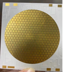
Ceramic AI2O3 Substrate Vender. Professional ALUMINUM AI2O3 packaging substrate production factory. BGA Ceramic AI2O3 base materials. we offer microtrace ALUMINUM AI2O3 substrates or PCBs.
In the realm of electronic packaging, ceramic packaging substrates emerge as vital foundations, especially for integrated circuits (ICs) and various electronic components. These substrates act as resilient canvases, streamlining the mounting and seamless interconnection of a wide array of electronic elements.
Outlined below are the salient characteristics and features that define ceramic packaging substrates:
Material Composition: Derived predominantly from compounds such as alumina (aluminum oxide) or aluminum nitride, ceramic packaging substrates exhibit remarkable traits. These encompass heightened thermal conductivity, sturdy mechanical resilience, and impeccable electrical insulation properties.
Thermal Conductivity: Ceramic substrates shine in their ability to conduct heat effectively, proficiently dissipating the thermal energy generated by electronic components. This capability is crucial for maintaining the enduring reliability and peak performance of electronic devices.
Electrical Insulation: Operating as adept electrical insulators, ceramics prevent undesirable electrical interactions among the diverse components on the substrate. This insulation prowess is pivotal for upholding the integrity of electronic circuits.
Dimensional Stability: Ceramic substrates boast commendable dimensional stability, maintaining their form and mechanical characteristics across diverse temperature and environmental scenarios. This stability is integral for the enduring reliability of electronic devices.
Hermetic Sealing: Endowed with adaptable design features, ceramic packaging substrates can provide hermetic sealing, creating a protective cocoon for delicate electronic components against environmental elements such as moisture and contaminants.
Thermal Expansion Matching: Engineers can tailor ceramic substrates to harmonize with the thermal expansion of other materials, mitigating stress induced by fluctuations in temperature.
Compatibility with Thin-Film Processes: Ceramic substrates seamlessly integrate with thin-film processes, showcasing versatility in the deposition of thin-film materials across a spectrum of electronic applications.
Ubiquitous in sectors where reliability, thermal efficiency, and electrical insulation take precedence—such as in power electronics, RF devices, sensors, and avant-garde electronic systems—the meticulous selection of ceramic material and substrate design aligns with the specific demands of electronic components and their intended applications.
What is the Function of Ceramic Packaging Substrate?
Ceramic packaging substrates act as dynamic facilitators, harmonizing a multitude of functions to guarantee the smooth operation of electronic devices.:
Structural Backbone: In the capacity of a robust base, ceramic packaging substrates provide indispensable structural support for the positioning of electronic components such as integrated circuits (ICs) and semiconductors. This foundational support is critical for maintaining the holistic integrity of electronic assemblies.
Heat Harmony: Tasked with efficient thermal dissipation, ceramic substrates leverage their high thermal conductivity to effectively disperse heat generated by electronic components. This capability is pivotal in preventing overheating and maintaining the reliable operation of electronic devices.
Electrical Insulation Mastery: Operating as adept electrical insulators, ceramic substrates prevent unwarranted electrical interactions between diverse components. This insulation proficiency is critical for ensuring the flawless functioning and integrity of electronic circuits.
Interconnection Maestro: Ceramic packaging substrates act as facilitators for the interconnection of varied electronic elements. They provide a strategic canvas for the placement of conductive traces and bonding wires, fostering seamless electrical connections between different components within the package.
Guardians of Environmental Resilience: Certain designs of ceramic substrates contribute to shielding electronic components from environmental elements. This may involve the implementation of hermetic sealing, establishing a protective fortress against moisture, contaminants, and external influences.
Dimensional Stability Artistry: Exhibiting commendable dimensional stability, ceramic substrates retain their form and mechanical properties across diverse temperature and environmental conditions. This stability is instrumental in ensuring the enduring reliability of electronic devices.
Versatility in Thin-Film Processes: The adaptability of ceramic substrates to thin-film processes adds a layer of versatility to their repertoire. This characteristic allows for the deposition of thin-film materials, expanding the horizons of applications for ceramic packaging substrates in the electronic landscape.
In essence, ceramic packaging substrates emerge as maestros in the symphony of electronic packaging, playing pivotal roles in providing structural support, managing heat dynamics, ensuring electrical insulation, facilitating interconnections, fortifying against environmental challenges, maintaining dimensional stability, and embracing the versatility of thin-film processes. Together, these functions harmonize to orchestrate the dependable performance and longevity of electronic devices.
What are the Different Types of Ceramic Packaging Substrate?
Ceramic packaging substrates present a rich array of types, each meticulously crafted to meet the intricate demands of electronic applications. These variants showcase distinct strengths in performance aspects, intricately designed to cater to a diverse spectrum of use cases:
Alumina (Aluminum Oxide) Substrates:Alumina substrates, held in high regard for their versatility, skillfully integrate thermal conductivity, electrical insulation, and mechanical strength. Whether empowering modules or enhancing LED packaging, they adeptly meet the diverse demands of a wide array of applications.
Aluminum Nitride (AlN) Substrates: Emerging as thermal conductive champions, AlN substrates outshine alumina, claiming a prominent role in applications where effective heat dissipation is crucial, particularly in high-power electronic devices.
Beryllium Oxide (BeO) Substrates: Boasting noteworthy thermal conductivity and a lightweight nature, BeO substrates deftly strike a nuanced equilibrium, their potential only tempered by safety considerations linked to the toxicity of beryllium.
Silicon Nitride (Si3N4) Substrates: Stepping to the forefront in settings that challenge with thermal shocks and demand steadfast mechanical strength, Si3N4 substrates shine in applications that necessitate durability in the face of both high temperatures and thermal cycling.
Fused Silica (SiO2) Substrates: Adopting a glass-like composition with low thermal expansion, fused silica substrates carve out a niche in applications seeking precision and stability amidst temperature fluctuations.
Zirconia (ZrO2) Substrates: Boasting high mechanical strength, toughness, and wear resistance, ZrO2 substrates confidently secure their place in applications where durability takes center stage.
Titanate Substrates: Crafted from titanate materials, these substrates delicately balance thermal conductivity and electrical insulation, finding resonance in applications where the harmonious interplay of these properties is pivotal.
Glass-Ceramic Substrates: Melding the characteristics of glass and ceramics, these substrates intricately harmonize thermal and electrical attributes. Their canvas extends to scenarios where insulation and effective heat dissipation merge into critical requirements.
The selection of a specific ceramic substrate type unfolds as a bespoke journey, guided by the nuanced demands of each application. Manufacturers respond with adept customization of material compositions and designs, ensuring a resplendent performance across the diverse landscapes of electronic applications.
How is Ceramic Packaging Substrate Connected to IC Packaging?
Ceramic packaging substrates weave a vital connection with IC (Integrated Circuit) packaging, acting as the linchpin in crafting a secure and dependable environment for semiconductor devices. The interplay between ceramic packaging substrates and IC packaging is intricate:
Foundational Anchorage: At its essence, ceramic packaging substrates serve as the bedrock for IC packaging, offering a robust foundation to anchor and shield integrated circuits and associated electronic components.
Thermal Choreography: Taking the lead in the intricate ballet of thermal management, ceramic substrates choreograph the efficient dissipation of heat generated by ICs. This dance prevents overheating, ensuring a seamless performance for semiconductor devices.
Electrical Isolation Artistry: Ceramic substrates showcase an artful mastery of electrical insulation. This proficiency is pivotal in preventing unintended interactions between components within the IC package, preserving the integrity of electronic circuits.
Conductive Canvas: Operating as a canvas for connectivity, ceramic substrates enable the artful interconnection of various components within the IC package. Precision placement of conductive traces and bonding wires ensures the creation of essential electrical connections.
Guardians of the Environment: Certain ceramic substrate designs assume the role of environmental guardians for ICs. This involves hermetic sealing, establishing a protective fortress against moisture, contaminants, and external elements that could jeopardize semiconductor devices.
Stalwart Dimensional Stability: The unwavering dimensional stability of ceramic substrates is a testament to their resilience, retaining form and mechanical properties across diverse temperatures and environmental conditions. This stability is instrumental for the enduring performance and reliability of ICs.
Thin-Film Tapestry: The adaptability of ceramic substrates to thin-film processes introduces an element of tapestry to IC packaging. This flexibility allows for the deposition of thin-film materials, broadening the creative palette for incorporating diverse materials and technologies.
In summary, ceramic packaging substrates stand as indispensable collaborators in IC packaging, providing not only structural support but contributing significantly to thermal regulation, electrical insulation, interconnection capabilities, environmental protection, dimensional stability, and the artistic versatility essential for the development of resilient and high-performance semiconductor devices.
What are the Differences Between Ceramic Packaging Substrate and PCB?
In the intricate tapestry of electronics, ceramic packaging substrates and PCBs (Printed Circuit Boards) emerge as pivotal players, each contributing its unique attributes. Let’s navigate the nuanced distinctions between these essential components:
Material Composition:
Ceramic Packaging Substrates: Crafted from ceramics like alumina, aluminum nitride, or beryllium oxide, boasting stellar thermal conductivity, electrical insulation, and mechanical fortitude.
PCBs: Forged from non-conductive materials like fiberglass-reinforced epoxy, featuring layered copper traces to orchestrate electrical conductivity.
Thermal Symphony:
Ceramic Packaging Substrates: Take the lead with a crescendo of high thermal conductivity, making them a natural choice for applications where the art of heat dissipation is paramount, especially in the realm of high-power electronics.
PCBs: Contribute to the melody with relatively lower thermal conductivity, occasionally harmonizing with additional measures like metal cores or heat sinks for enhanced thermal performance.
Electrical Ballet:
Ceramic Packaging Substrates: Showcase their balletic finesse in electrical insulation, gracefully preventing unintended interactions between electronic components.
PCBs: Dance primarily as conductors, relying on the choreography of the non-conductive substrate to ensure a seamless electrical performance.
Mechanical Resilience:
Ceramic Packaging Substrates: Project a robust stance in mechanical strength, providing a steadfast stage for the choreography of component mounting and ensuring enduring durability.
PCBs: Boast mechanical strength but may, at times, call for additional support structures to gracefully carry the weight of heavier components.
Cost Overture:
Ceramic Packaging Substrates: Tend to play a more elaborate overture in terms of costs, reflecting the nature of ceramic materials and the intricate manufacturing processes involved.
PCBs: Strike a more economical chord, contributing to their widespread presence across the diverse symphony of electronic applications.
Manufacturing Ballet:
Ceramic Packaging Substrates: Partake in a ballet of manufacturing processes like tape casting, co-firing, or thick-film printing, intricately woven into the fabric of ceramic craftsmanship.
PCBs: Engage in a dance of processes such as etching, drilling, and layer stacking, emblematic of the traditional manufacturing ballet in the world of PCBs.
Applications Symphony:
Ceramic Packaging Substrates: Ascend to the symphony’s crescendo in high-power electronic devices, RF applications, and scenarios demanding the virtuosity of superior thermal management.
PCBs: Embrace versatility, finding resonance across a spectrum of electronic devices, from the delicate notes of consumer electronics to the intricate melodies of computers and communication devices.
In essence, ceramic packaging substrates and PCBs navigate distinct movements in the electronic symphony, each attuned to specific needs. The choice between them is a dance dictated by the intricacies of the electronic composition, seeking the perfect harmony for optimal and resilient performance.
What is the Main Structure and Production Technology of Ceramic Packaging Substrate?
The architecture of a ceramic packaging substrate is a layered composition, intricately crafted through specialized production technologies tailored to the unique properties of ceramics. Let’s delve into the distinct structure and manufacturing processes that define ceramic packaging substrates:
Architectural Ensemble:
Fundamental Ceramic Stratum:
At the core lies the foundational layer, crafted from ceramic materials like alumina, aluminum nitride, beryllium oxide, or other ceramic compounds.
This stratum provides the necessary mechanical strength, forming a stable canvas for the integration of electronic components.
Conductive Pathways:
Delicate layers of conductive material, often metallic, are delicately etched onto the ceramic surface.
These pathways intricately weave the electrical connectivity, facilitating the symphony of electronic interactions.
Insulating Layers:
Dielectric layers are interwoven to insulate the conductive pathways, preventing electrical short circuits.
These layers play a crucial role in the electrical isolation of different components.
Metallized Coats:
Additional coats of metal, such as copper or aluminum, are applied to enhance electrical conductivity and foster seamless interconnections.
Via Passages:
Via passages, akin to portals, puncture the substrate, allowing vertical connections between various strata.
These conduits are filled with conductive material, forming the channels for electrical traversals.
Surface Elegance:
The topmost layer may receive a tailored finish, enhancing solderability and providing a hospitable surface for the affixation of electronic components.
Manufacturing Ballet:
Tape Casting Serenade:
Ceramic powders pirouette with binders in a graceful slurry, cast into thin tapes.
These tapes set the stage as the fundamental material for the substrate.
Layer Stacking Pas de Deux:
Layers of ceramic tapes perform a delicate dance, stacking in harmonious sequences to achieve the desired thickness.
The interplay of conductive and dielectric layers unfolds during this intricate choreography.
Lamination Sonata:
Stacked layers engage in a sonata of compression and lamination, merging into a harmonious structure.
Printed Poetry:
Conductive traces and patterns emerge like verses, painted onto the substrate with techniques such as screen printing or thick-film printing.
Dielectric materials join this poetic dance through similar artistic maneuvers.
Firing Overture (Co-Firing):
The substrate enters an overture of high-temperature firing, a grand symphony of sintering that solidifies the ceramic layers, imbuing them with density and mechanical strength.
Conductor materials undergo a metamorphosis, sintering into a seamless, continuous network.
Metallurgical Crescendo and Via Waltz:
Metallization layers take center stage through techniques like physical vapor deposition or chemical vapor deposition.
Via holes pirouette into existence, drilled or formed to create vertical connections, filled with conductive material in a waltz of connectivity.
Surface Finale:
The final act sees the surface adorned with a finishing touch, be it a solder mask or a protective coating.
Quality Symphony:
The entire performance is orchestrated under the watchful eyes of stringent quality control, ensuring the dimensional accuracy, electrical properties, and reliability of the ceramic packaging substrate.
This intricate dance of manufacturing processes culminates in the creation of a ceramic packaging substrate, a composition finely tuned to provide the requisite electrical, thermal, and mechanical characteristics for its role in electronic devices.
FAQs
What role do ceramic packaging substrates play in electronic devices?
Ceramic packaging substrates function as the fundamental support for mounting and interconnecting electronic components. Their roles encompass providing structural support, managing thermal conditions, ensuring electrical insulation, and furnishing a dependable platform for IC integration.
How are ceramic packaging substrates fabricated?
The manufacturing process involves a series of techniques such as tape casting, layer stacking, lamination, screen printing or thick-film printing, firing (co-firing), metallization, via formation, and surface finishing. These processes are tailored to ceramics to achieve specific and desired properties.
What are the advantages associated with the use of ceramic packaging substrates?
Advantages include high thermal conductivity, excellent electrical insulation, robust mechanical properties, dimensional stability, and suitability for applications involving high power and RF (Radio Frequency). Ceramic substrates are particularly valued for providing a reliable foundation for electronic component integration.
In which applications are ceramic packaging substrates commonly deployed?
Ceramic packaging substrates find application in diverse areas, including high-power electronic devices, RF and microwave components, power modules, LED packages, and other electronic systems where effective thermal management and reliability are critical.
How do ceramic packaging substrates differ from PCBs (Printed Circuit Boards)?
Ceramic packaging substrates differ from PCBs in terms of material composition, thermal conductivity, electrical properties, mechanical strength, and specific applications. While ceramic substrates excel in demanding thermal environments, PCBs offer versatility for general electronic applications.
Conclusion
In summary, ceramic packaging substrates emerge as the unsung heroes in the intricate realm of electronic packaging. They serve as the sturdy canvas upon which the electronic symphony is orchestrated, especially in the realm of integrated circuits (ICs). Crafted from advanced ceramic materials, these substrates boast a symphony of properties, including stellar thermal conductivity, mechanical robustness, electrical insulation, and unwavering dimensional stability.
The manufacturing journey of ceramic packaging substrates is akin to an intricate dance, involving tape casting, layer stacking, lamination, and a series of artistic steps like screen printing and firing. These processes, intricately tailored to the nuances of ceramics, bring forth substrates that meet the most discerning material requirements.
The advantages of employing ceramic packaging substrates unfold in applications demanding excellence—high-power electronics, RF and microwave components, power modules, and the luminosity of LED packages. Their stability and reliability, coupled with effective thermal management, position them as indispensable players in electronic systems where performance takes center stage.
Within the diverse array of ceramic packaging substrates, be it alumina, aluminum nitride, or silicon nitride, each type performs a unique sonata, catering to specific applications and performance benchmarks. Their distinct material properties add depth to the symphony of electronic design.
As we navigate the ever-evolving landscape of technology, the role of ceramic packaging substrates remains integral, providing a resilient stage for the electronic performance of the future. In this ongoing symphony, they stand as pillars of strength, shaping the harmonious future of electronic components and systems.