
Ceramic substrate/package manufacturing
Ceramic package substrates manufacturing, Ceramic PCB and Ceramic package substrates Vendor, we offer ceramic from 1 layer to 22 layers. Ceramic substrates/packages are essential components in electronic devices, providing a sturdy foundation for mounting and interconnecting various electronic components. Composed of ceramic materials such as alumina or aluminum nitride, these substrates offer superior thermal conductivity, electrical insulation, and mechanical strength. Their ability to efficiently dissipate heat makes them particularly suitable for high-power applications, ensuring reliable performance even in demanding environments. With customizable designs tailored to specific applications, ceramic substrates/packages accommodate diverse electronic configurations, including power modules, LED modules, RF amplifiers, and sensors. The manufacturing process involves precision shaping, printing of features like conductive traces and vias, firing to densify the ceramic material, and thorough quality testing to ensure reliability. Ceramic substrates/packages not only provide structural support but also contribute to the overall longevity and performance of electronic systems, making them indispensable components in modern technology.
What is a Ceramic Substrate/Package?
Ceramic substrate/package manufacturing and package substrate manufacturing. We use advanced Msap and Sap technology, High multilayer interconnection substrates from 4 to 18 layers,
A ceramic substrate/package is a component used in electronic packaging, particularly in semiconductor devices. It is made of ceramic materials such as alumina (Al2O3) or aluminum nitride (AlN) due to their excellent thermal conductivity, electrical insulation properties, and mechanical strength.
Ceramic substrates/packages serve as a platform for mounting and interconnecting various electronic components, including semiconductor chips, resistors, capacitors, and other active and passive devices. They provide electrical insulation and mechanical support while efficiently dissipating heat generated by the electronic components.
These packages come in various shapes and sizes depending on the specific application requirements. They often feature metal traces or vias for electrical connections and are commonly used in high-power applications, such as power modules, LEDs, radio frequency (RF) devices, and other high-performance electronic devices where thermal management is critical. Additionally, ceramic substrates/packages are favored in environments where reliability, durability, and resistance to harsh operating conditions are essential.
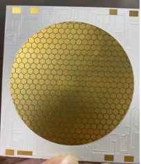
Ceramic Package Substrate
What are the Ceramic Substrate/Package Design Guidelines?
Design guidelines for ceramic substrate/package involve several considerations to ensure optimal performance, reliability, and manufacturability. Some key guidelines include:
- Thermal Management: Ensure adequate thermal management by incorporating features such as heat sinks, thermal vias, and thermal pads to efficiently dissipate heat from the electronic components.
- Material Selection: Choose ceramic materials with appropriate thermal conductivity, electrical insulation properties, and mechanical strength suitable for the specific application requirements.
- Dielectric Layer Thickness: Determine the optimal thickness of the dielectric layer to provide sufficient electrical insulation while minimizing parasitic capacitance and maximizing thermal conductivity.
- Interconnect Design: Design the interconnect layout to minimize signal propagation delay, reduce electromagnetic interference (EMI), and optimize signal integrity. This involves careful placement of signal traces, vias, and ground planes.
- Package Size and Shape: Select package size and shape based on the dimensions of the electronic components, as well as considerations for assembly, handling, and thermal performance.
- Assembly Considerations: Consider assembly processes such as wire bonding, flip-chip bonding, or soldering, and design the package accordingly to facilitate efficient and reliable assembly.
- Environmental Considerations: Account for environmental factors such as temperature fluctuations, humidity, and mechanical stress to ensure the package can withstand harsh operating conditions.
- Reliability Testing: Perform thorough reliability testing, including thermal cycling, mechanical shock, and vibration testing, to validate the robustness of the package design and ensure long-term reliability.
- Manufacturability: Design for manufacturability by considering factors such as material availability, cost-effectiveness, and compatibility with manufacturing processes such as screen printing, laser machining, and sintering.
- Documentation and Standards Compliance: Document the design specifications and ensure compliance with industry standards and regulations relevant to ceramic substrate/package manufacturing and electronic assembly processes.
By following these guidelines, designers can develop ceramic substrate/packages that meet performance requirements, exhibit high reliability, and are manufacturable at scale.
What is the Ceramic Substrate/Package Fabrication Process?
The fabrication process for ceramic substrates/packages typically involves several steps, including material preparation, shaping, printing, firing, and assembly. Here’s a general overview of the process:
- Material Preparation: The process begins with preparing the ceramic material, which is often alumina (Al2O3) or aluminum nitride (AlN). The raw materials are mixed, usually with binders and additives, to achieve the desired properties and consistency.
- Shaping: The prepared ceramic material is then shaped into the desired form, typically through methods such as dry pressing, tape casting, or injection molding. This step forms the green ceramic substrate/package in its initial shape.
- Printing: Various features such as conductive traces, vias, and insulating layers are printed onto the green ceramic substrate using techniques like screen printing or inkjet printing. Conductive materials like silver or gold paste are commonly used for printing conductive traces, while insulating materials may include dielectric pastes.
- Firing: The printed green ceramic substrate is fired in a kiln at high temperatures, typically between 1200°C to 1700°C, depending on the specific ceramic material used. This firing process removes the organic binders, densifies the ceramic material, and sintered the printed features to form a solid, rigid structure.
- Surface Finishing: After firing, the ceramic substrate/package may undergo surface finishing processes such as lapping, polishing, or metallization to achieve the desired surface smoothness and electrical properties.
- Assembly: Electronic components such as semiconductor chips, resistors, capacitors, and others are assembled onto the ceramic substrate using techniques like wire bonding, flip-chip bonding, or soldering. This step may also involve encapsulating the assembled components for protection.
- Testing and Quality Assurance: The finished ceramic substrate/packages undergo rigorous testing to ensure they meet the specified electrical, mechanical, and thermal performance requirements. This may include electrical testing, thermal cycling, and various reliability tests to assess long-term durability.
- Packaging and Shipping: Once the ceramic substrate/packages pass quality assurance, they are packaged and prepared for shipment to customers or further integration into electronic devices.
Throughout the fabrication process, quality control measures are implemented to ensure consistency and reliability of the ceramic substrate/packages, meeting the stringent requirements of various applications in industries such as automotive, aerospace, telecommunications, and consumer electronics.
How do you manufacture a Ceramic Substrate/Package?
Manufacturing a ceramic substrate/package involves several steps, as outlined below:
- Material Selection: Choose ceramic materials such as alumina (Al2O3) or aluminum nitride (AlN) based on the desired properties such as thermal conductivity, electrical insulation, and mechanical strength.
- Material Preparation: Raw materials are mixed with binders and additives to achieve the desired composition and consistency. This mixture is then shaped into green ceramic sheets or other forms using methods like dry pressing, tape casting, or injection molding.
- Printing: Various features such as conductive traces, vias, and insulating layers are printed onto the green ceramic substrate using techniques like screen printing or inkjet printing. Conductive materials like silver or gold paste are commonly used for printing conductive traces, while insulating materials may include dielectric pastes.
- Firing (Sintering): The printed green ceramic substrate is fired in a kiln at high temperatures, typically between 1200°C to 1700°C, depending on the specific ceramic material used. This firing process removes the organic binders, densifies the ceramic material, and sintered the printed features to form a solid, rigid structure.
- Surface Finishing: After firing, the ceramic substrate/package may undergo surface finishing processes such as lapping, polishing, or metallization to achieve the desired surface smoothness and electrical properties.
- Assembly: Electronic components such as semiconductor chips, resistors, capacitors, and others are assembled onto the ceramic substrate using techniques like wire bonding, flip-chip bonding, or soldering. This step may also involve encapsulating the assembled components for protection.
- Testing and Quality Assurance: The finished ceramic substrate/packages undergo rigorous testing to ensure they meet the specified electrical, mechanical, and thermal performance requirements. This may include electrical testing, thermal cycling, and various reliability tests to assess long-term durability.
- Packaging and Shipping: Once the ceramic substrate/packages pass quality assurance, they are packaged and prepared for shipment to customers or further integration into electronic devices.
Throughout the manufacturing process, quality control measures are implemented to ensure consistency and reliability of the ceramic substrate/packages, meeting the stringent requirements of various applications in industries such as automotive, aerospace, telecommunications, and consumer electronics.
How much should a Ceramic Substrate/Package cost?
The cost of a ceramic substrate/package can vary widely depending on several factors, including:
- Material: The type and quality of ceramic material used can significantly impact the cost. Higher-performance ceramics with superior thermal conductivity, electrical insulation, and mechanical strength may be more expensive.
- Size and Complexity: Larger and more complex substrates/packages require more material and manufacturing processes, leading to higher costs.
- Design Features: Features such as the number of layers, printed elements (traces, vias, etc.), surface finishing, and tolerances can influence the cost.
- Quantity: Economies of scale apply in manufacturing, so larger production runs typically result in lower per-unit costs.
- Manufacturing Processes: The specific manufacturing techniques employed, such as printing, firing, surface finishing, and assembly methods, can affect costs.
- Customization: Customized substrates/packages designed for specific applications may incur additional engineering and setup costs.
- Supplier and Location: Different suppliers may offer varying pricing structures, and manufacturing costs can also be influenced by factors such as labor costs and overhead expenses in different geographical locations.
As a rough estimate, ceramic substrates/packages can range in cost from a few dollars to several hundred dollars or more per unit, depending on the factors mentioned above. It’s essential for businesses to carefully evaluate their requirements and consider factors such as performance, reliability, and total cost of ownership when determining the budget for ceramic substrates/packages. Additionally, obtaining quotes from multiple suppliers and negotiating pricing based on volume and other factors can help optimize costs.
What is Ceramic Substrate/Package Base Material?
The base material of ceramic substrates/packages is typically a ceramic compound chosen for its specific properties suitable for electronic applications. The most common ceramic materials used as base materials for ceramic substrates/packages include:
- Alumina (Al2O3): Alumina is one of the most widely used ceramic materials for substrates/packages due to its excellent electrical insulation properties, high thermal conductivity, and mechanical strength. It is suitable for various applications, including power electronics, LED modules, and high-frequency circuits.
- Aluminum Nitride (AlN): Aluminum nitride offers even higher thermal conductivity compared to alumina, making it particularly suitable for applications requiring efficient heat dissipation, such as high-power LEDs, RF amplifiers, and power modules.
- Beryllium Oxide (BeO): Beryllium oxide possesses exceptionally high thermal conductivity, second only to diamond, making it ideal for applications requiring superior heat dissipation, such as high-power RF transmitters and microwave circuits. However, due to health and safety concerns associated with beryllium exposure, its use is restricted in certain regions.
- Silicon Nitride (Si3N4): Silicon nitride exhibits good thermal conductivity, excellent mechanical strength, and resistance to thermal shock, making it suitable for demanding applications in harsh environments, including automotive electronics and aerospace systems.
- Zirconia (ZrO2): Zirconia offers high mechanical strength, chemical resistance, and thermal stability, making it suitable for applications requiring durability and reliability in extreme conditions, such as sensor packaging and biomedical devices.
These ceramic materials are chosen based on their thermal conductivity, electrical insulation properties, mechanical strength, chemical stability, and compatibility with manufacturing processes to meet the specific requirements of electronic applications. Additionally, the choice of base material may also depend on factors such as cost, availability, and regulatory compliance.
Which company makes Ceramic Substrates/Packages? (Note: Our company can produce Ceramic Substrates/Packages)
Our company is equipped to manufacture high-quality ceramic substrates/packages tailored to meet specific requirements. With expertise in material selection, design, and fabrication processes, we ensure reliable and efficient ceramic solutions for electronic applications.
What are the 7 qualities of good customer service?
Good customer service involves various qualities that contribute to positive interactions and experiences for customers. Here are seven key qualities:
- Empathy: Understanding and empathizing with customers’ needs, concerns, and emotions is essential for providing effective support. Empathetic customer service representatives can build rapport, demonstrate care, and tailor solutions to meet individual customer needs.
- Patience: Patience is crucial when dealing with customers who may be frustrated, confused, or have complex issues. Customer service representatives should be able to listen attentively, remain calm, and take the time necessary to address concerns thoroughly.
- Clear Communication: Effective communication involves conveying information clearly and concisely, using language that is easy to understand and free of jargon. Customer service representatives should be able to explain products, policies, and solutions in a manner that is accessible and helpful to customers.
- Responsiveness: Being responsive means acknowledging customer inquiries or issues promptly and providing timely assistance or updates. Customers appreciate quick responses and proactive communication, even if a resolution may take time.
- Problem-Solving Skills: Customer service representatives should possess strong problem-solving skills to identify and resolve issues efficiently. This may involve critical thinking, resourcefulness, and the ability to think creatively to find solutions that meet customer needs.
- Professionalism: Maintaining professionalism in all interactions with customers is essential for building trust and credibility. This includes being courteous, respectful, and maintaining a positive attitude, regardless of the circumstances.
- Attention to Detail: Paying attention to detail ensures that customer inquiries or issues are addressed accurately and comprehensively. Customer service representatives should take care to gather relevant information, follow procedures correctly, and double-check solutions to avoid errors.
By embodying these qualities, businesses can deliver exceptional customer service experiences that foster customer satisfaction, loyalty, and positive word-of-mouth referrals.
FAQs (Frequently Asked Questions)
What is a ceramic substrate/package?
A ceramic substrate/package is a component used in electronic packaging, typically made of ceramic materials such as alumina or aluminum nitride. It provides mechanical support, electrical insulation, and thermal management for electronic components.
What are the advantages of using ceramic substrates/packages?
Ceramic substrates/packages offer excellent thermal conductivity, electrical insulation, and mechanical strength, making them ideal for high-power applications where efficient heat dissipation is crucial. They also provide reliability and durability in harsh operating environments.
What types of electronic devices use ceramic substrates/packages?
Ceramic substrates/packages are used in various electronic devices, including power modules, LED modules, RF amplifiers, sensors, and automotive electronics.
How are ceramic substrates/packages manufactured?
The manufacturing process typically involves material preparation, shaping, printing of features (such as conductive traces and vias), firing (sintering) to densify the ceramic material, surface finishing, assembly of electronic components, testing, and packaging.
What are the key properties to consider when selecting ceramic substrates/packages?
Important properties include thermal conductivity, electrical insulation, mechanical strength, thermal expansion coefficient, surface smoothness, and compatibility with assembly processes.
How do ceramic substrates/packages compare to other packaging materials, such as plastics or metals?
Ceramic substrates/packages offer superior thermal performance compared to plastics and metals, making them suitable for high-power applications. They also provide better electrical insulation and mechanical strength compared to most plastics.
What are the common failure mechanisms in ceramic substrates/packages?
Failure mechanisms may include thermal cycling-induced cracking, delamination of layers, solder joint fatigue, and mechanical stress from handling or assembly processes. Proper design, material selection, and reliability testing can help mitigate these risks.
Can ceramic substrates/packages be customized for specific applications?
Yes, ceramic substrates/packages can be customized in terms of size, shape, layer configuration, and feature layout to meet the requirements of specific applications.