
Extra small pitch PCB manufacturing
Extra Small Pitch PCB and Extra Small Pitch BGA substrates Manufacturing, We use high frequency and high speed materials to produce this extra small pitch PCB and packaging substrate from 2 layer to 22 layers. the best smallest pitch are 4mil.
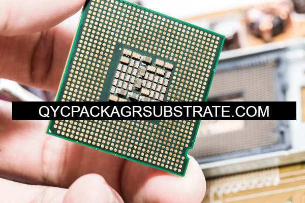
Extra Small Pitch PCBs, characterized by their closely spaced contact points, represent a pinnacle of miniaturization in electronic design. With a focus on optimizing space efficiency and signal integrity, these PCBs accommodate components with minimal separation between connection points, enabling the creation of incredibly compact electronic devices. Their small pitch allows for intricate routing of traces and facilitates the integration of high-density components, paving the way for advancements in areas such as consumer electronics, medical devices, and aerospace systems. Despite their diminutive size, Extra Small Pitch PCBs demand meticulous design and manufacturing processes to ensure reliable performance and adherence to strict tolerances. As a cornerstone of modern electronics, these PCBs exemplify the relentless pursuit of innovation in the quest for smaller, more powerful, and increasingly sophisticated electronic devices.
What is an Extra Small Pitch PCB?
Extra small pitch PCB manufacturing. the Package Substrate will be made with Showa Denko and Ajinomoto High speed materials.or other types high speed materials and high frequency materials.
An Extra Small Pitch PCB (Printed Circuit Board) refers to a PCB design where the distance between the center of one contact pad (such as a through-hole or surface mount component pad) to another is very small. “Pitch” in PCB design typically refers to the distance between the centers of adjacent contacts.
An Extra Small Pitch PCB would have a very tight arrangement of components, with contacts placed very close together. This type of design is often seen in compact electronic devices where space is at a premium, such as smartphones, wearables, IoT devices, and miniaturized electronics.
Designing and manufacturing Extra Small Pitch PCBs require precision in layout and manufacturing processes due to the reduced spacing between components. It often involves advanced techniques such as fine-pitch surface mount technology, high-density interconnects (HDI), and sometimes specialized fabrication methods to ensure reliable performance despite the small size and close proximity of components.
What are the Extra Small Pitch PCB Design Guidelines?
Designing Extra Small Pitch PCBs requires careful consideration of various factors to ensure proper functionality and manufacturability. Here are some guidelines typically followed:
- Component Selection: Choose components with small form factors whenever possible to minimize space usage. Use surface mount devices (SMDs) instead of through-hole components to save space and enable tighter packing.
- Layer Stackup: Optimize the layer stackup to accommodate the required routing density while maintaining signal integrity. Consider using high-density interconnect (HDI) technologies to increase routing density and reduce layer count.
- Routing Considerations:
– Minimize trace widths and spacings to accommodate the small pitch.
– Use microvias and blind vias to access inner layers without consuming excessive space.
– Maintain controlled impedance for critical signal traces.
– Ensure proper signal isolation and avoid signal crosstalk by careful routing and placement.
- Placement Guidelines:
– Place components strategically to minimize signal path lengths and reduce the complexity of routing.
– Consider thermal management and airflow to prevent overheating in densely packed areas.
– Ensure that components are placed within manufacturing tolerances to avoid assembly issues.
- Manufacturability:
– Verify that the design complies with the manufacturer’s capabilities and design rules.
– Ensure adequate solder mask clearances and keep in mind the limitations of solder mask registration.
– Check for any specific requirements regarding via sizes, annular ring sizes, and aspect ratios from the manufacturer.
- Testing and Validation:
– Perform thorough design rule checks (DRC) and electrical rule checks (ERC) to identify any potential issues.
– Prototype and test the design to validate functionality and performance before mass production.
- Documentation:
– Provide comprehensive documentation including assembly drawings, fabrication files, bill of materials (BOM), and assembly instructions to facilitate manufacturing and assembly processes.
- Compliance:
– Ensure that the PCB design complies with relevant industry standards and regulations, especially if the device will be used in safety-critical or regulated environments.
By following these guidelines, designers can create Extra Small Pitch PCBs that meet the requirements for functionality, reliability, and manufacturability in compact electronic devices.
Extra small pitch PCB
What is the Extra Small Pitch PCB Fabrication Process?
The fabrication process for an Extra Small Pitch PCB involves several steps, each crucial for achieving precision and reliability in the final product. Here’s a simplified overview of the process:
- Design Verification: Ensure the PCB design meets the specifications and requirements for the extra small pitch components. Check for proper clearances, trace widths, and other design parameters.
- Material Selection: Choose appropriate laminate materials based on the design requirements, such as FR-4, polyimide, or other specialized materials suited for fine-pitch applications.
- Panelization: Arrange multiple PCB designs into panels to optimize fabrication efficiency. Ensure proper spacing and alignment between individual PCBs within the panel.
- Photoresist Application: Coat the panel with a layer of photoresist material, which will be used to transfer the PCB pattern onto the substrate.
- Exposure: Expose the photoresist-coated panel to UV light through a photomask containing the PCB pattern. This step defines the copper traces and pads on the PCB.
- Development: Remove the unexposed photoresist using a developer solution, revealing the underlying copper traces and pads.
- Etching: Use chemical etchants to selectively remove the exposed copper, leaving behind the desired circuit pattern on the substrate.
- Surface Preparation: Clean the panel to remove any residues from the etching process and ensure proper adhesion of subsequent layers.
- Surface Finish Application: Apply a surface finish to protect the exposed copper traces and pads, and to enhance solderability. Common surface finishes include HASL, ENIG, OSP, and immersion tin.
- Solder Mask Application: Apply a solder mask over the entire panel, leaving openings for solder pads and vias. The solder mask protects the copper traces from oxidation and provides insulation between conductive elements.
- Silkscreen Printing: Print component designators, logos, and other markings onto the PCB surface using a silkscreen printing process. These markings aid in component placement and identification during assembly.
- Curing and Drying: Cure the panel in an oven to harden the solder mask and ensure proper adhesion. This step also removes any remaining solvents and moisture from the PCB.
- Routing and Singulation: Use a routing machine or mechanical saw to cut the panel into individual PCBs. Ensure precise cutting to avoid damage to the circuitry or components.
- Quality Control: Inspect the finished PCBs for defects such as shorts, open circuits, misalignments, or solder mask errors. Use automated optical inspection (AOI) or manual inspection techniques to verify quality.
- Packaging and Shipping: Package the finished PCBs securely to protect them during transit. Ship the PCBs to the assembly facility for component placement and soldering.
Throughout the fabrication process, strict quality control measures should be implemented to ensure that the Extra Small Pitch PCBs meet the required specifications for functionality, reliability, and manufacturability.
How do you manufacture an Extra Small Pitch PCB?
Manufacturing Extra Small Pitch PCBs requires specialized techniques and equipment to ensure precise placement and interconnection of components despite the small pitch. Here’s an overview of the manufacturing process:
- Design Verification: Before manufacturing begins, the PCB design undergoes thorough verification to ensure it meets all design requirements and guidelines for extra small pitch components.
- Material Selection: Select appropriate materials based on the design requirements, including the substrate material (typically FR-4 or more advanced materials for HDI boards), copper foil thickness, and solder mask materials.
- Panelization: Multiple PCBs are typically grouped together on a panel for simultaneous processing. Panelization helps optimize manufacturing efficiency.
- Laser Direct Imaging (LDI): LDI is often used for exposing the solder mask and creating the circuit pattern. It offers high precision, which is crucial for extra small pitch PCBs.
- Drilling and Plating: Microvias and through-holes are drilled into the PCB substrate, and then plated with conductive material to establish electrical connections between layers.
- Copper Plating and Etching: Copper layers are plated onto the substrate, and then etched away to form the desired circuit patterns.
- SMT Assembly: Surface Mount Technology (SMT) components are placed onto the PCB using pick-and-place machines. These machines precisely position components according to the design’s specifications.
- Reflow Soldering: The assembled PCBs undergo reflow soldering, where solder paste applied to the pads melts and creates the electrical connections between the components and the PCB.
- Inspection: Automated optical inspection (AOI) and X-ray inspection are commonly used to inspect the solder joints and ensure they meet quality standards.
- Testing: PCBs undergo functional testing to verify that all components are properly soldered, and the circuit functions as intended.
- Cleaning: PCBs are cleaned to remove flux residues and other contaminants left from the soldering process.
- Final Finishing: The PCBs may undergo final finishing processes such as surface finish application (e.g., HASL, ENIG, OSP) and routing to separate individual boards from the panel.
- Quality Assurance: Throughout the manufacturing process, quality control measures are implemented to ensure that each PCB meets the required specifications and standards.
- Packaging and Shipping: Once manufactured and inspected, the PCBs are packaged according to customer requirements and shipped to the end destination.
Manufacturing Extra Small Pitch PCBs requires precision at every step to ensure that the final product meets the demanding requirements of modern electronic devices.
How much should an Extra Small Pitch PCB cost?
The cost of an Extra Small Pitch PCB can vary widely depending on various factors such as:
- Board Size: Larger boards generally cost more due to the increased material and manufacturing requirements.
- Layer Count: Multilayer PCBs typically cost more than single or double-sided PCBs due to the complexity of fabrication.
- Complexity of Design: PCBs with intricate layouts, fine traces, and small pitch components may require specialized manufacturing processes, which can increase the cost.
- Materials: The choice of materials, such as laminate type and surface finish, can impact the cost of the PCB.
- Surface Finish: Different surface finishes come at different price points, with finishes like ENIG typically costing more than HASL or OSP.
- Quantity: Larger quantities often lead to lower per-unit costs due to economies of scale. However, prototype or low-volume production runs may have higher per-unit costs.
- Turnaround Time: Expedited fabrication services typically come at a premium compared to standard lead times.
- Additional Services: Services such as electrical testing, panelization, and component sourcing may incur extra costs.
Given these factors, it’s challenging to provide an exact cost without specific details about the PCB design, quantity, and manufacturing requirements. However, as a rough estimate, Extra Small Pitch PCBs might cost anywhere from a few dollars to several hundred dollars per square inch, depending on the complexity and volume of the order.
To get an accurate cost estimate, it’s best to consult with PCB manufacturers and provide them with detailed specifications of your design, including dimensions, layer count, materials, surface finish, and desired quantity. They can then provide a customized quote based on your requirements.
What is the Extra Small Pitch PCB base material?
The choice of base material for an Extra Small Pitch PCB depends on various factors such as the specific application, performance requirements, and manufacturing constraints. However, there are several common materials used as the base substrate for Extra Small Pitch PCBs:
- FR-4 (Flame Retardant-4): FR-4 is the most widely used substrate material for PCBs due to its affordability, availability, and good overall performance. It consists of woven fiberglass cloth impregnated with an epoxy resin. FR-4 PCBs are suitable for many applications, including those requiring extra small pitch components.
- High-Frequency Laminates: For applications involving high-frequency signals, such as RF and microwave circuits, specialized high-frequency laminates are used. These materials offer low dielectric constant (εr) and low loss tangent (tan δ), enabling better signal integrity at high frequencies. Examples include Rogers Corporation’s RO4000 series and Taconic’s TLY series.
- Polyimide (PI): Polyimide is a flexible substrate material suitable for applications requiring flexibility or high-temperature resistance. It is often used in flexible circuits or in applications where the PCB needs to withstand extreme environmental conditions.
- Rigid-Flex PCB Materials: Rigid-flex PCBs combine rigid and flexible substrates into a single board, offering both mechanical stability and flexibility. The rigid sections may use materials like FR-4, while the flexible sections typically use polyimide.
- Specialized Materials for HDI (High-Density Interconnect): HDI PCBs require materials with properties conducive to fine-pitch routing and microvia formation. These materials may include thin core laminates, build-up materials, and materials optimized for laser drilling.
When selecting the base material for an Extra Small Pitch PCB, it’s essential to consider factors such as electrical properties (dielectric constant, dissipation factor), mechanical properties (rigidity, flexibility), thermal properties, and cost. Additionally, ensure that the chosen material meets the specific requirements of the application and is compatible with the manufacturing processes involved in producing Extra Small Pitch PCBs.
Which company makes Extra Small Pitch PCBs?
There are many companies that specialize in manufacturing Extra Small Pitch PCBs, and these companies are typically professional PCB manufacturers or electronic manufacturing service providers. Some well-known companies include Foxconn, Omron, Hitachi Chemical, Samsung Electronics, and LG Electronics. These companies have advanced manufacturing equipment, professional engineering teams, and extensive experience to meet various customer demands for Extra Small Pitch PCBs.
As for our company, we are a professional electronic manufacturing service provider with advanced manufacturing equipment and experienced engineering team. We have the capability to produce various complex PCBs, including Extra Small Pitch PCBs. Our manufacturing processes and quality control procedures are stringent to ensure that the PCBs we produce meet the requirements and standards of our customers.
We are committed to providing customized solutions to our customers and designing and manufacturing Extra Small Pitch PCBs according to their specific requirements. We can offer professional advice and technical support based on our customers’ design requirements and technical specifications, and ensure the production of high-quality, reliable Extra Small Pitch PCBs. Our customers come from various industries such as communication, consumer electronics, medical, automotive, etc., and they are highly satisfied with our products and services.
In conclusion, our company has the technical capabilities, production equipment, and experience required to manufacture Extra Small Pitch PCBs, meeting various customer demands and providing high-quality, reliable products, and excellent service.
What are the 7 qualities of good customer service?
Good customer service is essential for building strong relationships with customers and fostering loyalty. Here are seven qualities that characterize good customer service:
- Responsiveness: Good customer service involves promptly addressing customer inquiries, concerns, and requests. Responding to customers in a timely manner demonstrates that their needs are valued and helps to build trust.
- Empathy: Empathy is the ability to understand and relate to the feelings and perspectives of customers. Effective customer service representatives listen actively, acknowledge customer concerns, and show genuine empathy in their interactions.
- Clear Communication: Clear and concise communication is crucial for providing excellent customer service. Customer service representatives should communicate information effectively, using language that is easy for customers to understand, and avoid jargon or technical terms that may confuse them.
- Problem-Solving Skills: Good customer service involves being proactive in resolving customer issues and finding solutions to their problems. Customer service representatives should be resourceful, patient, and capable of thinking critically to address customer needs effectively.
- Professionalism: Professionalism encompasses a range of qualities, including politeness, respectfulness, and integrity. Customer service representatives should conduct themselves professionally at all times, treating customers with courtesy and maintaining a positive attitude, even in challenging situations.
- Product Knowledge: Having a thorough understanding of the products or services offered is essential for providing helpful assistance to customers. Customer service representatives should be knowledgeable about the features, benefits, and usage of the products or services and be able to provide accurate information and guidance to customers.
- Consistency: Consistency is key to delivering a high level of customer service. Customers expect consistent experiences across all interactions with a company, whether online, over the phone, or in person. Consistency in service delivery helps to build trust and credibility with customers over time.
By embodying these qualities, businesses can deliver exceptional customer service experiences that not only meet but exceed customer expectations, leading to increased satisfaction, loyalty, and positive word-of-mouth recommendations.
FAQs
What are Extra Small Pitch PCBs?
Extra Small Pitch PCBs are printed circuit boards with closely spaced contact points, allowing for compact component placement and miniaturization of electronic devices. They are characterized by a small pitch, which refers to the distance between the centers of adjacent contacts.
What are the advantages of Extra Small Pitch PCBs?
Extra Small Pitch PCBs enable the design of smaller and more compact electronic devices, making them ideal for applications where space is limited. They also allow for increased routing density and improved signal integrity in high-speed applications.
What factors should be considered when designing Extra Small Pitch PCBs?
Designers need to consider factors such as component selection, routing density, layer stackup, signal integrity, thermal management, and manufacturability when designing Extra Small Pitch PCBs. Attention to detail is crucial to ensure the reliability and functionality of the final product.
What are the challenges in manufacturing Extra Small Pitch PCBs?
Manufacturing Extra Small Pitch PCBs requires advanced fabrication techniques and precision equipment to achieve tight tolerances and high levels of accuracy. Challenges may include fine-pitch soldering, precise alignment of components, and ensuring adequate signal isolation to prevent crosstalk.
What are some common applications of Extra Small Pitch PCBs?
Extra Small Pitch PCBs are used in a wide range of applications, including smartphones, tablets, wearables, IoT devices, medical devices, aerospace systems, and automotive electronics. Any application that requires miniaturization and high performance can benefit from Extra Small Pitch PCBs.
What are the design guidelines for Extra Small Pitch PCBs?
Design guidelines for Extra Small Pitch PCBs include minimizing trace widths and spacings, using high-density interconnect (HDI) technologies, optimizing component placement for efficient routing, and ensuring proper signal integrity and thermal management.
How can I find a reliable manufacturer for Extra Small Pitch PCBs?
Look for manufacturers with experience in producing Extra Small Pitch PCBs, advanced manufacturing capabilities, quality certifications, and a track record of delivering high-quality products. Request samples, ask for references, and inquire about their design and engineering support capabilities to ensure a successful partnership.