
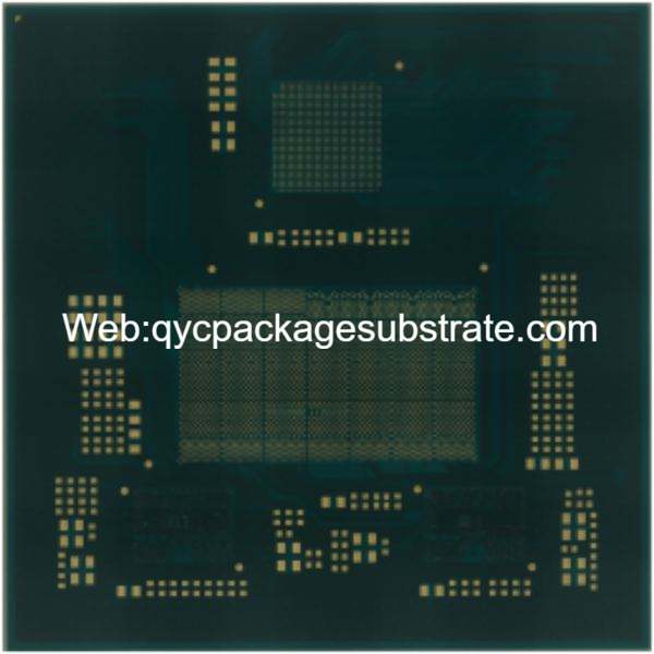
Flip-Chip Package Substrate manufacturer. the Package Substrate will be made with Showa Denko and Ajinomoto High speed materials.or other types high speed materials and high frequency materials.It is an electronic packaging technology that provides connection and support between electronic components and printed circuit boards. This technology “flips” an integrated circuit chip, turning it upside down and connecting it to a packaging substrate through microscopic solder joints. We mainly produce 10 to 18 layers small pitch Flip Chip Packaging Substrate. the best smallest Trace and spacing are 9um/9um. most of our customer has made the Trace and spacing with about 20um/20u. we can produce the 18 layers packaging substrate with any layers drilling.
What is a flip chip technology?
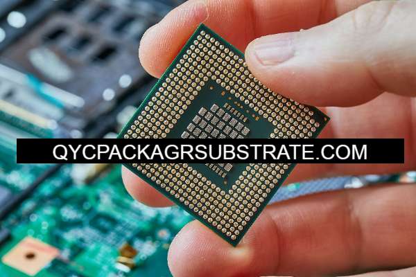
Flip Chip technology is a packaging method that during the packaging process, the electrical connection points of the chip are flipped down, aligned with and connected to the corresponding connection points on the packaging substrate.
This technology offers higher performance and density than traditional packaging methods because electrical connections are shorter and signals travel faster.
Composition of Flip Chip Packaging Substrate
Package Substrate: Typically a PCB or other type of substrate used to support and connect electronic components.
Flip Chip IC: An inverted integrated circuit chip with metal pads or balls for connection to the packaging substrate.
Underfill: An adhesive used to fill the gap between the chip and the package substrate, providing mechanical support and protection.
Advantages of Flip Chip Packaging
Electrical performance: Flip Chip technology provides faster signal transmission speeds and lower signal latency due to short-distance connections and lower inductance.
Thermal management: Due to the direct connection to the substrate, the heat of the chip can be dissipated more easily, providing better heat dissipation performance.
Size and weight: Flip chip packages are generally more compact, allowing the design of smaller, lighter electronic devices.
Reliability: Flip Chip connections are generally more durable because they are less susceptible to vibration and temperature changes.
Packaging substrate manufacturing process
The manufacturing process of Flip Chip Packaging Substrate typically involves multiple steps that require high precision and fine control to ensure the performance and reliability of electronic devices.
Substrate preparation
Select the substrate material: First, select the packaging substrate of an appropriate material, usually a PCB or other type of substrate. Material selection affects electrical performance, thermal management and mechanical strength.
Design Circuit: Design and layout the circuit on the substrate, including required connection points and required signal lines and power traces.
Preparing the Surface: Preparing the substrate surface usually involves removing any dirt, oxide, or grease to ensure reliable welding.
IC chip preparation
Flip Chip IC chip preparation: Prepare the IC chip to be connected, usually upside down, with metal pads or balls. These connection structures are usually made on the bottom of the chip.
Adhesive Application: Underfill is applied to the bottom of the chip or substrate to fill the gap between the chip and substrate and provide mechanical support. Adhesive selection and application must be precisely controlled.
Flip and position
Flip the chip: Turn the IC chip upside down so that its pads or balls face down, ready for connection to the substrate.
Positioning: Precisely positioning the inverted chip to the connection point on the substrate usually requires the use of high-precision positioning equipment.
Welding
Heat and pressure: Using heat and pressure, the pads or balls on the chip are soldered to the connection points on the substrate.
Welding temperature and time control: Welding temperature and time must be accurately controlled to ensure the quality of the solder joints and the reliability of the connection.
Packaging glue filling:
Encapsulant application: Encapsulant is applied to fill the gap between the chip and the substrate while avoiding the formation of bubbles and voids.
Curing: The encapsulant needs to be cured, usually using thermal curing or UV curing methods.
Testing and Inspection
Electrical Performance Testing: Connected chips and substrates may require electrical performance testing to ensure proper connections and no shorts or opens.
Appearance inspection: Check the appearance to ensure the quality of solder joints and packaging glue.
Finished product processing
Trim: Trim remaining joining material or encapsulant as needed.
Marking: For tracking and identification purposes, marking information may need to be added to the substrate.
Encapsulation and integration
Once completed, the packaging substrate can be integrated into a larger electronic device, often requiring it to be placed within a housing to protect the internal components.
Packaging substrate application areas
Flip Chip Packaging Substrate is widely used in various fields, especially in electronic devices that require high performance, high density, reliability and thermal management.
Computers and Microprocessors
In high-performance computers and servers, flip chip packages are commonly used in microprocessors and GPUs. These applications require high-speed signal transmission, excellent thermal performance and compact packaging.
Flip Chip technology can provide faster signal transmission speed and lower signal delay, thereby enhancing computer performance.
Communication device
In mobile phones, network equipment and communication base stations, Flip Chip packaging is used for RF modules, baseband processors and other communication chips.
Because Flip Chip connection can reduce inductance and provide higher frequency response, it is suitable for high-frequency communications.
Consumer Electronics
Flip Chip packaging is widely used in consumer electronics products such as smartphones, tablets, digital cameras and game consoles.
These applications often require compact packaging and high performance while minimizing product size.
Flip Chip Packaging Substrate
Vehicle electronics
In the field of automotive electronics, Flip Chip Packaging Substrate is used to manufacture automotive control units, embedded systems and sensors.
The high temperature and vibration environment inside the vehicle requires connection stability and reliability.
Medical equipment
Medical devices, such as medical imaging equipment, implantable devices, and implantable medical devices, often use flip chip packaging to provide highly integrated solutions.
Aerospace and Defense
In aerospace and defense applications, Flip Chip Packaging Substrate is used to manufacture advanced spacecraft, missiles, radar systems and military communications equipment.
In summary, Flip Chip Packaging Substrate is widely used in various electronic devices that require high performance, high density, reliability and thermal management. As technology continues to develop, its use in different application areas continues to expand.
Package substrate design considerations
Thermal management
Heat dissipation design: Provide sufficient heat dissipation for the Flip Chip IC chip to ensure that the heat can be effectively dissipated. This can include heat sinks, thermal pads and thermal design.
Thermal expansion matching: Consider the thermal expansion coefficients of the substrate material and chip material to avoid thermal stress issues.
Signal integrity:
Electrical design: Ensure impedance matching of signal transmission lines and control the length of signal lines to reduce signal distortion.
Signal line spacing: Maintain sufficient signal line spacing to reduce crosstalk and mutual interference.
EMC
Shielding design: Use appropriate shielding technology to reduce the impact of electromagnetic interference on surrounding circuits.
Grounding strategy: Ensure good grounding to reduce the spread of electromagnetic noise.
Mechanical stability and reliability
Strength design: Ensure that the packaging substrate has sufficient mechanical strength to withstand transportation, vibration and impact.
Environmental tolerance: Consider the environmental conditions to which the device may be subjected, such as humidity, temperature changes, and chemicals, to ensure long-term reliability.
Manufacturing feasibility
Manufacturing process requirements: PCB manufacturing process requirements should be considered when designing, such as minimum line width, spacing, and minimum aperture.
Component Assembly: Ensure that the design of the packaging substrate allows components to be mounted and connected accurately and reliably.
Standard compliance
Comply with relevant standards: Ensure designs comply with relevant industry standards and specifications to ensure product reliability and compliance.
Advantages and disadvantages of packaging substrates
Flip Chip Packaging Substrate, as a packaging technology, has various advantages and some limitations. The following is their detailed description:
Advantage
Shorter signal path: Flip Chip flips the chip onto the substrate, reducing the length of the signal path, thereby reducing signal transmission delay and improving circuit performance.
Higher performance: Due to shorter signal paths and tighter circuit layout, Flip Chip packaging provides higher performance, including higher clock frequencies and lower power consumption.
Better heat dissipation: Flip Chip technology connects the chip directly to the substrate for better heat transfer, lowering chip temperature, helping to prevent overheating and maintain long-term reliability.
Smaller package size: Flip Chip chip packages are generally more compact than traditional packages, which helps reduce device size, especially for mobile devices and embedded systems.
Increased input/output density: Because the connection to the chip is direct, Flip Chip technology allows more input/output pins to be placed on the same area, which contributes to richer functionality and higher data throughput.
Shortcoming
Complex manufacturing process: Flip Chip packaging requires a more complex manufacturing process, including precise positioning and connection control, which can increase production costs.
Reliability issues: Due to the complexity of the packaging process, Flip Chip packages may be more susceptible to soldering and connection issues that can lead to reliability issues such as broken or shorted electrical connections.
Difficult to Repair: Once the chip is flipped and connected, it becomes very difficult to repair the fault or replace the chip, which can be a challenge for devices in need of repair.
Higher Cost: Flip Chip packaging is generally more expensive than traditional packaging due to complexity and manufacturing technology requirements.
Not Compatible with Certain Applications: Due to its performance and reliability characteristics, the Flip Chip package is not suitable for all applications. and maintenance difficulties.
Packaging substrate material and structures
Material
Organic substrate:
FR-4: This is one of the most common organic substrate materials and is typically made from fiberglass-reinforced epoxy resin. It has good insulating properties and is suitable for most general purpose applications.
PI: PI substrates have excellent high temperature stability and chemical stability, so they are often used in high-performance applications such as aerospace and high-speed communication equipment.
BT: BT substrate is suitable for high-frequency applications and has good dielectric properties and low loss characteristics.
Inorganic substrate
Ceramic Substrate: Typically made of Al2O3, ceramic substrates have excellent thermal conductivity and dielectric properties and are suitable for high-power applications.
Silicon Substrate: Silicon substrate is commonly used in microelectronic packaging, especially MEMS and sensors.
Other materials: ABF series, Rogers series, high frequency and high speed materials.
Structure
The structure of the packaging substrate can vary depending on the application and design needs, but typically includes the following components:
Package Substrate Core: This is the main part of the substrate that supports and connects the chips. The core is usually constructed of materials such as FR-4, PI, BT, ceramic or silicon.
Copper Layer: A layer of copper is applied to the core to create electrical connections. Copper layers are usually divided into inner and outer layers. The inner copper layer connects to the chip pins through holes, and the outer copper layer is used to connect other electronic components such as resistors, capacitors, and connecting lines.
Dielectric layer: The dielectric layer is used to isolate the copper layer and prevent short circuits between circuit components. The dielectric layer is typically constructed of fiberglass-reinforced epoxy or other insulating material.
Metal Layer: The metal layer is usually on the outside and is used to connect the substrate to external circuitry or a heat sink. These metal layers typically include pads and pins.
Drilling and via connections: Drilling holes connect the inner and outer copper layers to create electrical connections between chip pins and external components. These hole connections are often coated with a conductive coating to provide connectivity.
Components: Depending on the application needs, the packaging substrate may also include other components such as capacitors, inductors, resistors and connecting lines.
Confirm the production and delivery process
Order Acceptance and Specification Confirmation: The customer places the order and the manufacturer confirms the specifications and requirements.
Raw material procurement: Procurement of required substrate materials and other raw materials.
Design and Engineering: Engineers design circuit layouts and component placement.
Material preparation: Prepare substrate material and attach copper foil.
Manufacturing Production: Manufacture of circuit boards, including circuit routing and assembly of components.
Testing and quality control: Conduct electrical performance and reliability testing to ensure product quality.
Packaging and Labeling: Pack the product into standard packaging suitable for shipping and label it.
Delivery: Negotiate delivery details with customers, deliver products to customers, and customer acceptance.
Summary
Flip Chip technology is a method in which the electrical connection points of the chip are flipped down during the packaging process, aligned with and connected to the corresponding connection points on the packaging substrate. It provides higher performance and density. Flip Chip Packaging Substrate consists of a packaging substrate (usually a PCB), an inverted chip, and an Underfill used to fill the gap between the chip and the substrate. The advantages of Flip Chip Packaging include faster signal transmission, superior thermal management, compact size and weight, and higher reliability. It is widely used in computers, communications, consumer electronics, automobiles, medical equipment, aerospace and defense and other fields. Design considerations for package substrates need to consider thermal management, signal integrity, EMC, mechanical stability and reliability, as well as manufacturing feasibility and standards compliance. Packaging substrate materials and structural materials include organic substrates (such as FR-4, PI, BT) and inorganic substrates (such as ceramics and silicon). The structure usually includes the packaging substrate core, copper layer, dielectric layer and metal layer.
FQAs
Q: What is Flip Chip Packaging Substrate?
A: Flip Chip Packaging Substrate is an electronic packaging technology that provides connection and support for electronic components by turning the integrated circuit chip upside down and connecting it to the packaging substrate through tiny solder joints.
Q: How is Flip Chip technology different from traditional packaging?
A: Flip Chip technology is different from traditional packaging methods because it flips the chip’s electrical connection points downward to directly align and connect with the connection points on the packaging substrate. This reduces signal path length, improving performance and density.
Q: What are the advantages of Flip Chip Packaging Substrate?
A: The advantages of Flip Chip Packaging Substrate include faster signal transmission, superior thermal management, compact size and lightweight, and higher reliability. It is particularly useful in high-performance and high-density applications.
Q: In what application fields is Flip Chip technology common?
A: Flip Chip technology is commonly used in computers, communications equipment, consumer electronics, automotive electronics, medical equipment, aerospace and defense, and other fields. It is suitable for applications requiring high performance, high density, reliability and thermal management.