
Micro via PCB manufacturing
Micro via PCB manufacturing. the best smallest via holes size are 50um(0.05mm). the best smallest trace are 9um. the best smallest gap are 9um. we have made the Micro via PCBs from 4 layer to 20 layers. to use the High frequency and high speed materials.
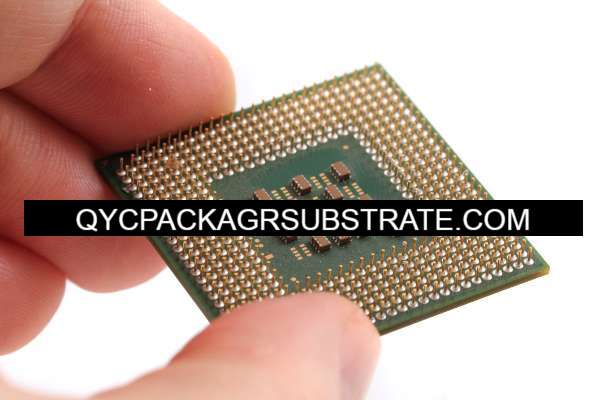
Micro via PCBs revolutionize electronic device design by enabling higher-density interconnects in smaller spaces. These PCBs incorporate tiny diameter vias, typically less than 150 micrometers, facilitating intricate layer-to-layer connections. This technology allows for compact designs without compromising functionality or performance. With micro via PCBs, manufacturers can achieve significant miniaturization, making them ideal for applications where space is limited, such as smartphones, tablets, wearable devices, and IoT gadgets. The reduced size and increased routing density enhance signal integrity, enabling faster data transfer and improved overall performance. Additionally, micro via PCBs offer better thermal management and weight reduction benefits, contributing to the efficiency and durability of electronic devices. Overall, micro via PCBs represent a cutting-edge solution for achieving high-density, high-performance circuitry in today’s increasingly compact electronic devices.
What is a Micro via PCB?
Micro via PCB manufacturing and package substrate manufacturing. We use advanced Msap and Sap technology, High multilayer interconnection substrates from 4 to 18 layers,
A micro via PCB (Printed Circuit Board) refers to a type of PCB design that incorporates very small diameter vias. Vias are essentially small holes in a PCB that are used to connect different layers of the board. These connections allow for the transfer of signals or power between the different layers, enabling the PCB to function as intended.
Micro vias are typically defined as vias with diameters smaller than 150 micrometers. They are used in high-density interconnect (HDI) PCB designs where space is at a premium and where traditional through-hole vias or even standard-sized blind and buried vias are not feasible due to size constraints.
Micro via PCBs offer several advantages, including:
- Increased Density: Micro vias allow for tighter packing of components and interconnects, enabling designers to fit more functionality into a smaller footprint.
- Improved Signal Integrity: With shorter signal paths and reduced parasitic effects, micro vias can help improve signal integrity and reduce signal loss, especially in high-frequency applications.
- Enhanced Thermal Management: Micro vias can aid in heat dissipation by providing more efficient paths for thermal transfer between layers.
- Reduced Weight: By allowing for thinner PCBs and smaller components, micro via technology can help reduce the overall weight of electronic devices, which is crucial in applications where weight is a concern, such as aerospace or automotive industries.
However, it’s important to note that the fabrication of micro via PCBs requires advanced manufacturing techniques and specialized equipment, which can increase production costs compared to traditional PCBs. Additionally, the design and layout considerations for micro via PCBs can be more complex, requiring careful planning to ensure signal integrity and reliability.
Micro via PCB manufacturing
What are Micro via PCB Design Guidelines?
Micro via PCB design guidelines are a set of recommendations and best practices to follow when designing a PCB that incorporates micro vias. These guidelines help ensure the manufacturability, reliability, and performance of the PCB. Here are some common micro via PCB design guidelines:
- Minimum Via Size: Determine the minimum acceptable diameter for micro vias based on manufacturing capabilities and requirements. Typically, micro vias have diameters smaller than 150 micrometers.
- Aspect Ratio: Consider the aspect ratio (ratio of the depth to the diameter) of micro vias to ensure they can be reliably manufactured. Keep the aspect ratio within acceptable limits to prevent issues such as plating voids or barrel cracking.
- Pad Size: Ensure that the pad sizes for micro vias are appropriately sized to provide sufficient copper coverage and adhesion during plating processes. Pad sizes should be designed to accommodate the micro via diameter and any required annular ring.
- Keepout Zones: Define keepout zones around micro vias to prevent interference with adjacent components or signal traces. Maintain adequate clearance between micro vias and other PCB features to avoid electrical and mechanical issues.
- Layer Stacking: Plan the layer stacking configuration carefully, considering the placement of micro vias and their relationship to signal traces and component pads on adjacent layers. Optimize layer stacking to minimize signal crosstalk and impedance discontinuities.
- Annular Rings: Ensure that micro vias have sufficient annular rings (the copper pad around the via hole) to maintain electrical connectivity and mechanical stability. Follow recommended guidelines for annular ring width based on the micro via diameter.
- Thermal Considerations: Account for thermal management requirements when placing micro vias, especially in high-power or high-density applications. Ensure adequate spacing and distribution of vias to facilitate heat dissipation and prevent localized hot spots.
- Signal Integrity: Optimize the layout of micro vias to minimize signal reflections, impedance mismatches, and other signal integrity issues. Maintain consistent trace widths and spacing to preserve signal integrity across the PCB.
- Design for Manufacturability (DFM): Collaborate closely with PCB manufacturers to ensure that the design meets their manufacturing capabilities and requirements. Considerations such as panelization, solder mask application, and via plating processes should be addressed during the design phase.
- Testing and Inspection: Implement provisions for testing and inspection of micro vias during PCB fabrication to verify their quality and reliability. Conduct electrical testing and visual inspection to detect any defects or irregularities that could affect performance.
By adhering to these micro via PCBs design guidelines, designers can optimize the performance, reliability, and manufacturability of their PCBs, especially in applications requiring high-density interconnects and miniaturization.
What is the Micro via PCB Fabrication Process?
The fabrication process for micro via PCBs involves several steps, including design, material selection, drilling, plating, etching, and inspection. Here’s a general overview of the micro via PCB fabrication process:
- Design: The PCB design process begins with the creation of the circuit schematic and layout using PCB design software. Designers specify the location, size, and routing of micro vias according to the requirements of the PCB design.
- Material Selection: Select the appropriate substrate material for the PCB based on factors such as electrical properties, thermal conductivity, and mechanical strength. High-quality materials such as FR-4, polyimide, or ceramic are commonly used for micro via PCBs.
- Drilling: Micro vias are drilled into the substrate using advanced drilling techniques such as laser drilling or mechanical drilling with specialized micro drills. Laser drilling is often preferred for its precision and ability to create smaller diameter vias with high aspect ratios.
- Desmear and Etchback: After drilling, the substrate undergoes desmear and etchback processes to remove any debris or resin smear generated during drilling. Desmear removes excess resin from the drilled holes, while etchback controls the depth of the vias.
- Lamination: Multiple layers of prepreg (pre-impregnated resin) and copper foil are laminated together to form the multilayer PCB stack-up. The layers are compressed and bonded under heat and pressure to create a solid, uniform structure.
- Copper Plating: Copper is electroplated onto the walls of the drilled vias to provide electrical conductivity and interlayer connections. Copper plating also forms the conductive traces and pads on the outer layers of the PCB.
- Pattern Plating: Through a series of photolithography and etching steps, the desired circuit patterns are defined on the outer layers of the PCB. Pattern plating involves selectively depositing and etching copper to create the conductive traces and pads according to the PCB design.
- Surface Finish: Apply a surface finish to protect the exposed copper surfaces and improve solderability. Common surface finishes for micro via PCBs include immersion gold, HASL (Hot Air Solder Leveling), ENIG (Electroless Nickel Immersion Gold), and OSP (Organic Solderability Preservative).
- Solder Mask and Legend Printing: Apply solder mask over the PCB surface to insulate and protect the conductive traces, leaving openings for component pads and vias. Legend printing is used to add component designators, logos, and other markings to the PCB surface.
- Final Inspection: Perform a series of quality control checks and inspections to verify the dimensional accuracy, electrical continuity, and overall quality of the finished PCB. Automated optical inspection (AOI) and electrical testing are commonly used for quality assurance.
- Routing and Singulation: After inspection, the PCB panels are routed and singulated into individual PCBs according to the desired dimensions and specifications. Precision routing equipment is used to cut the panels along the defined board outlines.
- Packaging and Shipping: Once singulated, the finished PCBs are packaged and prepared for shipping to the customer or assembly facility for component mounting and soldering.
Throughout the micro via PCB fabrication process, strict quality control measures are implemented to ensure that the finished PCBs meet the required specifications for performance, reliability, and functionality. Collaboration between PCB designers, manufacturers, and quality assurance teams is essential to achieve successful fabrication of micro via PCBs.
How do you manufacture a Micro via PCB?
Manufacturing a micro via PCB involves several specialized processes to create the intricate interconnects and compact designs required for high-density electronic applications. Here’s a step-by-step overview of the manufacturing process for micro via PCBs:
- Design and Layout: The PCB design begins with the creation of the circuit schematic and layout using specialized PCB design software. Designers specify the location, size, and routing of micro vias according to the requirements of the PCB design, taking into account factors such as signal integrity, thermal management, and component placement.
- Material Selection: Select the appropriate substrate material for the PCB based on factors such as electrical properties, thermal conductivity, and mechanical strength. High-quality materials such as FR-4, polyimide, or ceramic are commonly used for micro via PCBs.
- Drilling: Micro vias are drilled into the substrate using advanced drilling techniques such as laser drilling or mechanical drilling with specialized micro drills. Laser drilling is often preferred for its precision and ability to create smaller diameter vias with high aspect ratios.
- Desmear and Etchback: After drilling, the substrate undergoes desmear and etchback processes to remove any debris or resin smear generated during drilling. Desmear removes excess resin from the drilled holes, while etchback controls the depth of the vias.
- Lamination: Multiple layers of prepreg (pre-impregnated resin) and copper foil are laminated together to form the multilayer PCB stack-up. The layers are compressed and bonded under heat and pressure to create a solid, uniform structure.
- Copper Plating: Copper is electroplated onto the walls of the drilled vias to provide electrical conductivity and interlayer connections. Copper plating also forms the conductive traces and pads on the outer layers of the PCB.
- Pattern Plating: Through a series of photolithography and etching steps, the desired circuit patterns are defined on the outer layers of the PCB. Pattern plating involves selectively depositing and etching copper to create the conductive traces and pads according to the PCB design.
- Surface Finish: Apply a surface finish to protect the exposed copper surfaces and improve solderability. Common surface finishes for micro via PCBs include immersion gold, HASL (Hot Air Solder Leveling), ENIG (Electroless Nickel Immersion Gold), and OSP (Organic Solderability Preservative).
- Solder Mask and Legend Printing: Apply solder mask over the PCB surface to insulate and protect the conductive traces, leaving openings for component pads and vias. Legend printing is used to add component designators, logos, and other markings to the PCB surface.
- Final Inspection: Perform a series of quality control checks and inspections to verify the dimensional accuracy, electrical continuity, and overall quality of the finished PCB. Automated optical inspection (AOI) and electrical testing are commonly used for quality assurance.
- Routing and Singulation: After inspection, the PCB panels are routed and singulated into individual PCBs according to the desired dimensions and specifications. Precision routing equipment is used to cut the panels along the defined board outlines.
- Packaging and Shipping: Once singulated, the finished PCBs are packaged and prepared for shipping to the customer or assembly facility for component mounting and soldering.
Throughout the micro via PCB manufacturing process, strict quality control measures are implemented to ensure that the finished PCBs meet the required specifications for performance, reliability, and functionality. Collaboration between PCB designers, manufacturers, and quality assurance teams is essential to achieve successful fabrication of micro via PCBs.
How much should a Micro via PCB cost?
The cost of manufacturing a micro via PCB can vary widely depending on several factors, including the complexity of the design, the number of layers, the size of the board, the quantity ordered, the choice of materials and surface finishes, and the manufacturing processes involved. However, here are some general considerations to keep in mind when estimating the cost of micro via PCBs:
- Complexity of the Design: PCBs with intricate designs, high-density interconnects, and micro vias may require specialized manufacturing processes and equipment, which can increase the cost.
- Number of Layers: The number of layers in the PCB stack-up affects the manufacturing complexity and material cost. More layers typically result in higher manufacturing costs.
- Size of the Board: Larger PCBs require more material and may incur additional manufacturing costs. Conversely, smaller PCBs may be more cost-effective to produce.
- Quantity Ordered: Economies of scale apply in PCB manufacturing, meaning that larger production quantities can result in lower per-unit costs. Ordering larger quantities upfront can help reduce the cost per board.
- Choice of Materials: The type of substrate material, copper thickness, and surface finish selected for the PCB can impact the overall cost. High-quality materials and finishes may come with a higher price tag.
- Surface Finish: Different surface finishes such as immersion gold, HASL, ENIG, or OSP have varying costs associated with them. The choice of surface finish depends on the specific requirements of the application and the budget.
- Lead Time: Shorter lead times may incur expedited manufacturing fees, which can increase the overall cost of the PCBs.
- Additional Services: Additional services such as assembly, testing, and conformal coating may incur extra charges.
To get an accurate cost estimate for your specific micro via PCB project, it’s recommended to consult with multiple PCB manufacturers and provide them with detailed specifications, including the PCB design files, quantity required, desired lead time, and any additional requirements. The manufacturers can then provide quotes based on your specific project parameters.
What is Micro via PCB base material?
The base material for micro via PCBs, also known as substrate material, plays a crucial role in determining the performance, reliability, and manufacturability of the PCB. Several types of materials can be used as the base material for micro via PCBs, each offering different properties and characteristics. Some common base materials for micro via PCBs include:
- FR-4 (Flame Retardant-4): FR-4 is a widely used epoxy-based laminate material reinforced with woven glass fiber. It offers good electrical insulation properties, mechanical strength, and dimensional stability. FR-4 is suitable for a wide range of applications and is often chosen for its cost-effectiveness.
- Polyimide (PI): Polyimide is a high-temperature-resistant polymer that is well-suited for applications requiring excellent thermal stability, flexibility, and resistance to harsh environments. Polyimide-based substrates are commonly used in flexible PCBs and applications where thermal management is critical.
- Rogers Materials: Rogers Corporation offers a range of high-performance laminate materials specifically designed for RF/microwave applications. These materials provide low dielectric loss, tight dielectric constant control, and excellent high-frequency performance, making them ideal for micro via PCBs used in wireless communication systems, radar systems, and other high-frequency applications.
- Ceramic Substrates: Ceramic materials such as alumina (Al2O3) and aluminum nitride (AlN) offer excellent thermal conductivity, mechanical strength, and stability at high temperatures. Ceramic substrates are commonly used in high-power electronic devices and applications requiring efficient thermal management.
- Metal Core Substrates: Metal core substrates, also known as metal core PCBs (MCPCBs), feature a metal base layer (typically aluminum or copper) sandwiched between layers of dielectric material. These substrates offer enhanced thermal conductivity and heat dissipation, making them suitable for high-power LED lighting, automotive electronics, and power electronics applications.
The choice of base material for micro via PCBs depends on factors such as the specific requirements of the application, the operating environment, thermal management needs, signal integrity considerations, and budget constraints. Designers should carefully evaluate the properties and characteristics of different base materials to select the most suitable option for their micro via PCB design. Collaboration with PCB manufacturers and material suppliers can also provide valuable insights into material selection based on their expertise and experience.
Which company makes Micro via PCB?
Micro via PCBs are produced by many specialized PCB manufacturing companies, some of which are dedicated to the research and production of high-density interconnect technology and micro via processes. There are many well-known PCB manufacturers worldwide, such as Taiwan’s TAIYO ELECTRONICS, America’s Molex, South Korea’s KB PCB, and Japan’s Hitachi Chemical Co., Ltd. These companies have rich experience in the PCB field and advanced manufacturing equipment to provide high-quality micro via PCBs to meet customer needs.
As for our company, we have advanced PCB manufacturing processes and technologies to produce high-quality micro via PCBs. Our manufacturing facility is equipped with advanced equipment, including precision laser drilling machines, automated production lines, and quality inspection devices. Our engineering team has extensive experience and can provide professional technical support and customized solutions to meet specific customer requirements.
We are committed to continuously improving our technical capabilities and production capacity to ensure that we provide customers with high-quality products and services. We strictly adhere to international standards and quality management systems to ensure that our products meet customer requirements and industry standards.
Whether in the fields of communication, medical, aerospace, automotive electronics, or industrial control, we have extensive experience and successful cases. We understand the importance of micro via PCBs in modern electronic products, so we strive to continuously improve our production capacity and product quality to meet the growing demands of customers.
In conclusion, our company has the technical strength, manufacturing capabilities, and professional experience required to produce micro via PCBs. We will continue to work hard to provide customers with high-quality, reliable micro via PCBs and collaborate with them to create a better future.
What are the 7 qualities of good customer service?
Good customer service is essential for building strong relationships with customers and ensuring their satisfaction. Seven qualities of good customer service include:
- Responsiveness: A good customer service representative should respond promptly to customer inquiries, concerns, and requests. Being responsive demonstrates attentiveness and a commitment to addressing customers’ needs in a timely manner.
- Empathy: Empathy involves understanding and acknowledging the emotions and perspectives of customers. Good customer service representatives empathize with customers’ situations, show compassion, and strive to resolve issues with sensitivity and understanding.
- Clarity: Providing clear and concise communication is crucial for effective customer service. Good customer service representatives communicate information, instructions, and solutions in a clear and understandable manner, avoiding confusion and misunderstanding.
- Professionalism: Good customer service is characterized by professionalism, which includes maintaining a positive attitude, adhering to company policies and procedures, and conducting oneself with integrity and respect towards customers.
- Problem-Solving Skills: Good customer service representatives possess strong problem-solving skills to effectively address customer concerns and resolve issues. They identify root causes, offer viable solutions, and follow through to ensure customer satisfaction.
- Patience: Dealing with customers, especially those who may be upset or frustrated, requires patience and composure. Good customer service representatives remain calm, listen attentively, and demonstrate patience while assisting customers, even in challenging situations.
- Consistency: Consistency in customer service is important for building trust and reliability. Good customer service representatives strive to deliver consistent service experiences to all customers, ensuring that each interaction reflects the company’s values and standards.
By embodying these qualities, organizations can provide exceptional customer service that fosters loyalty, enhances reputation, and contributes to long-term success.
FAQs (Frequently Asked Questions)
What are Micro via PCBs?
Micro via PCBs are printed circuit boards that incorporate very small diameter vias for high-density interconnects. These vias, typically less than 150 micrometers in diameter, enable the connection of different layers within the PCB, allowing for compact and complex designs.
What are the benefits of using Micro via PCBs?
Micro via PCBs offer several advantages, including increased density, improved signal integrity, enhanced thermal management, reduced weight, and miniaturization of electronic devices. They are particularly useful in applications requiring high-density packaging and miniaturization.
What is the difference between Micro vias and traditional vias?
Micro vias are significantly smaller in diameter compared to traditional vias, which allows for higher routing densities and finer pitch designs. Traditional vias are larger and are typically used for through-hole connections or standard buried and blind vias.
What are the key considerations in designing Micro via PCBs?
Designing Micro via PCBs requires careful consideration of factors such as minimum via size, aspect ratio, pad size, layer stacking, annular ring size, thermal management, and signal integrity. Attention to these factors ensures manufacturability, reliability, and optimal performance.
What manufacturing processes are involved in producing Micro via PCBs?
The manufacturing process for Micro via PCBs includes drilling, desmear and etchback, lamination, copper plating, pattern plating, surface finish application, solder mask, legend printing, final inspection, routing, and singulation. These processes require specialized equipment and expertise to produce high-quality Micro via PCBs.
What applications are suitable for Micro via PCBs?
Micro via PCBs are used in a wide range of applications, including consumer electronics, telecommunications, aerospace, medical devices, automotive electronics, and industrial controls. They are particularly beneficial in high-frequency and high-speed applications, as well as miniaturized electronic devices.
How can I ensure the quality of Micro via PCBs?
To ensure the quality of Micro via PCBs, it is essential to work with reputable PCB manufacturers who have expertise in Micro via technology. Additionally, thorough design verification, adherence to industry standards, and rigorous quality control measures during manufacturing are crucial for producing high-quality Micro via PCBs.