
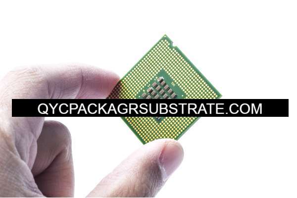
Microvias | Blind Vias PCB manufacturing
Microvias | Blind Vias PCB manufacturing. We cand do the best smallest via holes size are 50um with Blind and buried via holes HDI PCBs from 2 layer to 20 layers.
Microvias | Blind Vias PCBs represent an advanced technology in printed circuit board design, facilitating intricate connections and compact layouts for modern electronic devices. Microvias are tiny drilled holes, often less than 150 micrometers in diameter, enabling connections between different layers of the PCB. Meanwhile, blind vias connect the outer layers of the board to one or more inner layers without traversing the entire thickness.
These specialized vias offer several advantages, including enhanced signal integrity, reduced signal distortion, and the ability to accommodate high-density interconnects. By enabling more efficient use of PCB real estate, Microvias | Blind Vias PCBs contribute to the miniaturization of electronic devices while maintaining or improving performance.
Designing Microvias | Blind Vias PCBs requires careful consideration of factors such as minimum annular ring size, aspect ratio, trace spacing, and thermal management. Additionally, selecting appropriate base materials and surface finishes is crucial to ensure optimal electrical and mechanical properties.
Overall, Microvias | Blind Vias PCBs represent a sophisticated solution for demanding applications where space constraints, signal integrity, and reliability are paramount. Their adoption continues to drive innovation in various industries, from consumer electronics to aerospace and beyond.
What is a Microvias | Blind Vias PCB?
Microvias | Blind Vias PCB manufacturingHigh speed and high frequency material packaging substrate manufacturing. Advanced packaging substrate production process and technology
A microvia is a small drilled hole in a printed circuit board (PCB) that is typically less than 150 micrometers in diameter. Microvias are used to connect different layers of the PCB together, allowing for more complex routing of traces and reducing the overall size of the board.
Blind vias, on the other hand, are drilled holes that connect the outer layers of a PCB to one or more inner layers, but do not go all the way through the entire board. This means that blind vias are visible from only one side of the PCB.
A PCB that incorporates both microvias and blind vias is often referred to as a “Microvias | Blind Vias PCB.” This type of PCB allows for high-density interconnects and can be used in applications where space is limited and signal integrity is crucial, such as in high-speed digital devices or mobile electronics. The combination of microvias and blind vias enables designers to create more compact and complex PCB layouts while maintaining signal integrity and reliability.
Microvias | Blind Vias PCB manufacturing
What are the Microvias | Blind Vias PCB Design Guidelines?
Here are some general design guidelines for Microvias | Blind Vias PCBs:
- Minimum Annular Ring: The annular ring is the copper pad around the drilled hole. It’s recommended to maintain a minimum annular ring width to ensure reliable electrical connections. Typically, this width should be at least 3-4 mils (0.076-0.1 mm).
- Aspect Ratio: The aspect ratio is the ratio of the PCB thickness to the diameter of the drilled hole. For microvias, the aspect ratio should typically be kept below 1:1 to ensure reliable manufacturing and plating processes.
- Minimum Trace Spacing: Ensure an adequate spacing between traces and vias to prevent electrical interference and short circuits. The minimum trace spacing depends on various factors like the PCB fabrication process, the dielectric material used, and the required electrical characteristics.
- Layer Stacking: Plan the layer stackup carefully to optimize signal integrity and impedance control. Consider the signal paths and the distribution of power and ground planes to minimize signal distortion and noise.
- Via Placement: Strategically place vias to minimize signal distortion and impedance mismatches. Use vias sparingly and avoid excessive via stubs that can introduce signal reflections and degrade signal quality.
- Thermal Considerations: Consider thermal management requirements, especially for high-power applications. Distribute vias evenly to improve heat dissipation and avoid localized hot spots on the PCB.
- Manufacturing Constraints: Be aware of the manufacturing capabilities and limitations of your PCB fabrication vendor. Consult with them early in the design process to ensure that your design can be manufactured reliably and cost-effectively.
- Design for Testing: Include test points and access vias in your design to facilitate testing and troubleshooting during production and assembly.
- Signal Integrity Analysis: Perform signal integrity analysis using simulation tools to verify the electrical performance of your design, especially for high-speed digital signals.
- Documentation and Communication: Clearly document your design guidelines and communicate them effectively with your PCB fabrication vendor and assembly partner to ensure that your design requirements are understood and implemented correctly.
By following these guidelines, you can design Microvias | Blind Vias PCBs that meet your electrical, mechanical, and manufacturability requirements effectively.
What is the Microvias | Blind Vias PCB Fabrication Process?
The fabrication process for Microvias | Blind Vias PCBs involves several key steps:
- Design: The PCB design is created using PCB design software. Design considerations include layer stackup, trace routing, via placement, and other factors specific to Microvias and Blind Vias.
- Preparation of Substrate: The substrate material, typically a laminate consisting of layers of fiberglass and epoxy resin, is prepared. The substrate is cut to the desired size and cleaned to remove any contaminants.
- Drilling: Microvias and Blind Vias are drilled into the substrate using precision drilling equipment. For Microvias, which are small in diameter, lasers or mechanical drills with fine drill bits are used. Blind Vias are drilled partially through the substrate to connect the outer layers with one or more inner layers.
- Desmear and Clean: After drilling, the substrate undergoes a desmear process to remove any debris or smear left from the drilling process. This step ensures good adhesion of the copper plating to the substrate.
- Copper Plating: Copper is deposited onto the walls of the drilled holes through a process called electroplating. This forms the conductive pathways for the vias. The thickness of the copper plating is controlled to meet design requirements.
- Dry Film Lamination: A layer of dry film photoresist is applied to the substrate, covering the copper-plated vias. This film is then exposed to UV light through a photomask, which defines the desired circuit pattern.
- Development and Etching: The exposed areas of the dry film photoresist are removed using a developing solution, leaving behind the circuit pattern. The substrate is then etched to remove the exposed copper, leaving behind the desired copper traces and vias.
- Surface Finish: Surface finish processes such as HASL (Hot Air Solder Leveling), ENIG (Electroless Nickel Immersion Gold), or OSP (Organic Solderability Preservatives) are applied to protect the exposed copper surfaces and facilitate soldering during assembly.
- Solder Mask Application: A layer of solder mask is applied over the copper traces and vias, leaving only the desired areas exposed for soldering. The solder mask provides protection from environmental factors and prevents solder bridges during assembly.
- Silkscreen Printing: Component designators, logos, and other markings are printed onto the PCB using a silkscreen printing process.
- Final Inspection and Testing: The finished PCBs undergo visual inspection, electrical testing, and other quality control measures to ensure they meet the specified requirements.
Once the fabrication process is complete, the PCBs are ready for assembly, where components are soldered onto the board to create the final electronic assembly.
How do you manufacture a Microvias | Blind Vias PCB?
Manufacturing a Microvias | Blind Vias PCB involves a specialized fabrication process due to the complexity of creating small drilled holes and blind vias. Here’s an overview of the manufacturing process:
- Design Preparation: The PCB design is created or modified to incorporate Microvias and Blind Vias. This includes defining the layer stackup, determining the location and size of vias, and optimizing trace routing.
- Substrate Preparation: The base substrate material, typically a laminate composed of layers of fiberglass and epoxy resin, is prepared. It is cut to the desired size and cleaned to remove any contaminants that could affect the fabrication process.
- Drilling Microvias and Blind Vias: Precision drilling equipment is used to create Microvias and Blind Vias in the substrate. Microvias are small diameter holes drilled completely through the substrate, while Blind Vias are drilled partially through the substrate to connect the outer layers with one or more inner layers. Laser drilling or mechanical drilling with fine drill bits is commonly used for Microvias, while specialized drilling techniques are employed for Blind Vias.
- Desmear and Clean: After drilling, the substrate undergoes a desmear process to remove any debris or smear left from the drilling process. This step is crucial for ensuring good adhesion of the subsequent copper plating.
- Copper Plating: Copper is deposited onto the walls of the drilled holes through electroplating. This forms the conductive pathways for the vias. The thickness of the copper plating is controlled to meet design requirements, typically using multiple plating steps to achieve the desired thickness.
- Dry Film Lamination and Imaging: A layer of dry film photoresist is applied to the substrate, covering the copper-plated vias. This film is then exposed to UV light through a photomask, defining the desired circuit pattern. The exposed areas are then developed and etched to remove excess copper, leaving behind the desired traces and vias.
- Surface Finish Application: Surface finish processes such as HASL (Hot Air Solder Leveling), ENIG (Electroless Nickel Immersion Gold), or OSP (Organic Solderability Preservatives) are applied to protect the exposed copper surfaces and facilitate soldering during assembly.
- Solder Mask Application: A layer of solder mask is applied over the copper traces and vias, leaving only the desired areas exposed for soldering. The solder mask provides protection from environmental factors and prevents solder bridges during assembly.
- Silkscreen Printing: Component designators, logos, and other markings are printed onto the PCB using a silkscreen printing process.
- Final Inspection and Testing: The finished PCBs undergo visual inspection, electrical testing, and other quality control measures to ensure they meet the specified requirements.
Once the manufacturing process is complete, the PCBs are ready for assembly, where components are soldered onto the board to create the final electronic assembly.
How much should a Microvias | Blind Vias PCB cost?
The cost of manufacturing a Microvias | Blind Vias PCB can vary significantly depending on various factors such as:
- Board Size: Larger PCBs typically cost more due to increased material usage and manufacturing complexity.
- Number of Layers: The number of layers in the PCB affects the fabrication process complexity and material cost.
- Complexity of Design: Designs with intricate routing, fine pitch components, and high-density interconnects may require specialized manufacturing processes, which can increase costs.
- Type of Material: Different substrate materials have varying costs. High-performance materials with special properties may be more expensive than standard FR-4.
- Aspect Ratio of Vias: Higher aspect ratio vias (ratio of hole depth to diameter) may require additional manufacturing steps, increasing costs.
- Surface Finish: The choice of surface finish (e.g., HASL, ENIG, OSP) can impact cost due to differences in material and processing requirements.
- Volume: Larger production runs typically result in lower per-unit costs due to economies of scale.
- Turnaround Time: Expedited manufacturing services may incur additional charges.
- Supplier and Location: PCB fabrication costs can vary between different manufacturers and regions due to labor costs, equipment capabilities, and other factors.
To get an accurate cost estimate for your specific Microvias | Blind Vias PCB project, it’s best to consult with PCB fabrication vendors and provide them with detailed design specifications. They can offer quotes based on your requirements and provide insights into cost-saving measures or alternative options to meet your budget constraints.
What is Microvias | Blind Vias PCB base material?
The base material for Microvias | Blind Vias PCBs typically consists of a substrate made of fiberglass reinforced epoxy resin, commonly known as FR-4 (Flame Retardant 4). FR-4 is widely used in the electronics industry for its excellent electrical insulation properties, mechanical strength, and affordability.
However, for specialized applications requiring higher performance, different base materials may be used. Some examples include:
- High-Speed Applications: For high-speed digital applications where signal integrity is critical, materials like FR-4 with higher glass transition temperatures (Tg) or specialized laminates such as Rogers or Isola materials may be used. These materials offer better electrical properties and reduced signal loss at high frequencies.
- High-Frequency Applications: For RF/microwave circuits operating at extremely high frequencies, substrates with low dielectric constant (Dk) and low loss tangent (Df) are preferred. Materials like PTFE (Polytetrafluoroethylene) or ceramic-filled laminates are commonly used in such applications.
- Thermal Management: In applications where thermal management is important, substrates with high thermal conductivity may be used. Aluminum-based or metal-core PCBs provide efficient heat dissipation compared to traditional FR-4.
The choice of base material depends on the specific requirements of the application, including electrical performance, thermal management, mechanical stability, and cost considerations. It’s essential to select a suitable base material that meets the design criteria and performance specifications of the Microvias | Blind Vias PCB.
Which company makes Microvias | Blind Vias PCB?
Microvias | Blind Vias PCBs are highly complex printed circuit boards (PCBs) commonly used in high-density interconnect and sophisticated electronic devices. At present, many PCB manufacturing companies are capable of producing Microvias | Blind Vias PCBs to meet the demands of various industries.
These companies employ precise manufacturing processes and advanced technologies to produce Microvias | Blind Vias PCBs. They have professional engineering teams and experienced technicians capable of providing comprehensive services from design to production. These companies also collaborate closely with supply chain partners to ensure high-quality raw materials are obtained and stringent quality control is maintained throughout the production process.
As a PCB manufacturing company with extensive experience and expertise, our company is also capable of producing Microvias | Blind Vias PCBs. We have state-of-the-art production equipment and technology and are committed to continuously improving our manufacturing processes to meet customers’ demands for high-quality PCBs.
Our engineering team can customize designs according to customer requirements and provide professional advice and support. We strictly adhere to international standards and industry regulations to ensure that the produced PCBs have excellent electrical performance, reliability, and stability.
Through our dedication and commitment, our company can meet customers’ needs for Microvias | Blind Vias PCBs and provide high-quality, reliable products and services. We will continue to strive for improvement and innovation to meet the evolving market demands and provide better solutions for our customers.
What are the 7 qualities of good customer service?
Good customer service is characterized by several key qualities that contribute to positive interactions and relationships with customers. Here are seven qualities of good customer service:
- Responsiveness: Good customer service involves being prompt and responsive to customer inquiries, concerns, and requests. Customers appreciate timely assistance and expect their needs to be addressed promptly.
- Empathy: Empathy is the ability to understand and share the feelings of customers. Good customer service representatives empathize with customers’ situations, acknowledge their emotions, and demonstrate genuine concern for their needs.
- Clear Communication: Effective communication is essential for good customer service. Clear and concise communication helps customers understand information, instructions, and solutions provided by the service representative.
- Professionalism: Professionalism involves maintaining a courteous and respectful demeanor when interacting with customers. Good customer service representatives conduct themselves professionally at all times, regardless of the situation or customer behavior.
- Knowledgeability: Customers expect service representatives to have the knowledge and expertise necessary to address their questions and resolve their issues. Good customer service involves being well-informed about products, services, policies, and procedures.
- Problem-Solving Skills: Good customer service representatives possess strong problem-solving skills to address customer concerns and resolve issues effectively. They are resourceful, proactive, and committed to finding solutions that meet customers’ needs.
- Follow-Up and Accountability: Good customer service extends beyond initial interactions. It involves following up with customers to ensure their needs have been met satisfactorily and taking accountability for any promises made or commitments given during the interaction.
By embodying these qualities, organizations can provide exceptional customer service experiences that foster customer satisfaction, loyalty, and positive word-of-mouth referrals.
FAQs
What are Microvias and Blind Vias in PCB design?
Microvias are small drilled holes in a PCB, typically less than 150 micrometers in diameter, used to connect different layers of the PCB. Blind vias are drilled holes that connect the outer layers of a PCB to one or more inner layers without going through the entire board.
What are the advantages of using Microvias and Blind Vias?
Microvias and Blind Vias enable high-density interconnects, allowing for more compact PCB designs. They also improve signal integrity and reduce signal distortion in high-speed digital circuits.
What factors should be considered when designing Microvias | Blind Vias PCBs?
Designers should consider factors such as minimum annular ring size, aspect ratio, trace spacing, layer stacking, via placement, thermal management, manufacturing constraints, and signal integrity analysis.
What materials are commonly used for Microvias | Blind Vias PCBs?
The base material for Microvias | Blind Vias PCBs is typically FR-4 (Flame Retardant 4), but specialized materials may be used for high-frequency or high-performance applications.
What is the fabrication process for Microvias | Blind Vias PCBs?
The fabrication process involves steps such as design, substrate preparation, drilling, copper plating, dry film lamination, development and etching, surface finish, solder mask application, silkscreen printing, and final inspection and testing.
Which companies manufacture Microvias | Blind Vias PCBs?
Many PCB manufacturing companies offer Microvias | Blind Vias PCB fabrication services. Customers can choose a reputable manufacturer based on factors such as experience, capabilities, quality standards, and cost.
How much does a Microvias | Blind Vias PCB cost?
The cost of a Microvias | Blind Vias PCB depends on factors such as board size, number of layers, complexity of design, type of material, volume, turnaround time, and supplier. It’s best to consult with PCB fabrication vendors for accurate cost estimates based on specific project requirements.