
Minimum Clearance BGA Circuit Board Manufacturer
Minimum Clearance BGA Circuit Board Manufacturer,Minimum Clearance BGA Circuit Boards are designed to accommodate Ball Grid Array (BGA) packages with minimal spacing between solder balls and the PCB surface. This design allows for high-density packaging and efficient use of space, making them ideal for compact, high-performance electronics. The board’s layout requires precise alignment and meticulous manufacturing to ensure reliable soldering and optimal electrical connections. Typically used in applications such as mobile devices, consumer electronics, and advanced computing systems, minimum clearance BGA circuit boards support high-speed data transmission and enhanced signal integrity while maximizing board real estate. Their design helps meet the demands of modern, space-constrained electronic devices.
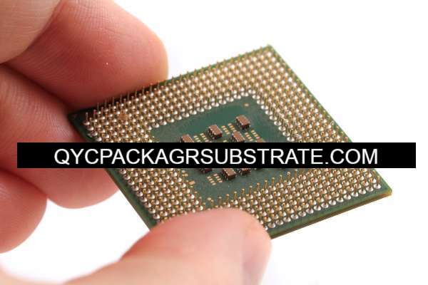
What is a Minimum Clearance BGA Circuit Board?
A Minimum Clearance BGA (Ball Grid Array) Circuit Board is a specialized type of printed circuit board designed to accommodate BGA components with very tight spacing between the solder balls and traces. BGAs are a popular type of surface-mount packaging used in electronics due to their high-density connections and improved electrical performance. However, as the size of these packages continues to shrink and the number of pins increases, the challenge of managing space and maintaining performance becomes more complex.
In a Minimum Clearance BGA PCB, the layout is engineered to achieve the smallest possible distance between the BGA pads and adjacent traces or other components. This tight clearance is critical for high-density designs where real estate on the board is limited. Achieving minimum clearance requires precise manufacturing techniques and high-quality materials to ensure reliable performance and durability.
Several factors contribute to the design and production of minimum clearance BGA circuit boards, including advanced PCB fabrication processes, specialized soldering techniques, and high-resolution imaging systems. These factors help to ensure that the small clearances do not compromise the integrity of the electrical connections or the mechanical stability of the components.
The benefits of minimum clearance BGA PCBs include reduced board size, increased functionality, and improved signal integrity, making them suitable for applications in consumer electronics, telecommunications, and high-performance computing. However, they also pose challenges in terms of heat dissipation and assembly accuracy, requiring careful consideration during both design and manufacturing stages.
Minimum Clearance BGA Circuit Board Manufacturer
What are the Design Guidelines for Minimum Clearance BGA Circuit Boards?
Designing Minimum Clearance BGA (Ball Grid Array) Circuit Boards requires careful consideration to ensure both reliability and performance, given the tight spacing constraints. Here are key design guidelines to follow:
- Pad and Trace Design: Ensure that pad sizes are correctly specified for the BGA balls to facilitate proper soldering. The traces routed near the pads should be kept as short as possible and positioned to avoid interference with the BGA pads.
- Clearance Rules: Adhere to strict clearance rules between the BGA pads and adjacent traces or components. This includes maintaining adequate space to prevent solder bridging and ensuring that soldering processes do not cause electrical shorts.
- Thermal Management: Implement efficient thermal management strategies. BGA packages can generate significant heat, and tight clearances can exacerbate thermal issues. Use thermal vias and heat sinks as necessary to dissipate heat and maintain component performance.
- Signal Integrity: Design with signal integrity in mind. High-speed signals can be affected by crosstalk and impedance mismatches, especially in tightly spaced layouts. Use controlled impedance traces and proper grounding to maintain signal quality.
- Manufacturing Tolerances: Design with manufacturing tolerances in mind. Ensure that your design accounts for the capabilities of the PCB manufacturer to avoid issues such as misalignment and soldering defects due to tight clearances.
- Testing and Inspection: Implement robust testing and inspection protocols. Use advanced imaging systems and inspection techniques to verify that the board meets the minimum clearance requirements and that solder joints are properly formed.
- Design for Assembly: Consider the assembly process. Ensure that the design facilitates accurate placement and soldering of BGA components, reducing the risk of defects due to misalignment or inadequate solder flow.
- Simulation and Prototyping: Utilize simulation tools to model the performance of the BGA layout, including thermal and electrical simulations. Build prototypes to validate the design and make necessary adjustments before final production.
By adhering to these guidelines, you can design Minimum Clearance BGA PCBs that offer high performance and reliability despite the challenges of tight spacing.
What is the Fabrication Process for Minimum Clearance BGA Circuit Boards?
The fabrication process for Minimum Clearance BGA (Ball Grid Array) Circuit Boards involves several precise steps to ensure high-quality production despite the tight spacing constraints. Here’s an overview of the key steps:
- Design and Layout: The process begins with a detailed design and layout of the PCB, including the BGA component placements and minimum clearance requirements. Advanced design tools are used to ensure that pad sizes, trace routing, and clearances are optimized for the specific BGA package and its pin configuration.
- PCB Material Preparation: The PCB substrate is selected based on the design requirements, typically involving materials that can handle fine traces and high-density components. Common materials include FR-4, high-frequency laminates, or other specialized substrates depending on the application.
- Photolithography: A photolithographic process is used to create the circuit pattern on the PCB substrate. This involves applying a photosensitive coating (photoresist) to the board, exposing it to ultraviolet light through a mask that defines the circuit pattern, and then developing the exposed photoresist to reveal the underlying copper layer.
- Etching: After photolithography, the exposed copper areas are etched away using chemical solutions, leaving behind the desired circuit pattern. This step is critical for creating fine traces and pads with minimal clearance.
- Drilling and Plating:Holes are drilled for through-hole components and vias. These holes are then plated with copper to create electrical connections between different layers of the PCB. Precision drilling and plating are essential to avoid damaging delicate traces and to ensure accurate hole sizes.
- Solder Mask Application: A solder mask is applied to protect the PCB’s copper traces and pads from solder bridging and contamination. The solder mask is applied over the entire board except for the areas where soldering is needed, such as BGA pads.
- Surface Finish: A surface finish is applied to the exposed pads to improve solderability. Common finishes include HASL (Hot Air Solder Leveling), ENIG (Electroless Nickel Immersion Gold), or OSP (Organic Solderability Preservative). The choice of finish can impact the reliability and performance of the solder joints.
- BGA Pad Preparation: For minimum clearance BGA boards, the pads and solder mask openings are meticulously prepared to accommodate the tight spacing. Special attention is given to the accuracy of pad dimensions and alignment to ensure proper soldering of BGA components.
- Inspection and Testing: The fabricated PCBs undergo rigorous inspection and testing to ensure that they meet design specifications. This includes visual inspection, automated optical inspection (AOI), and electrical testing to verify that all connections are intact and that there are no defects.
- Assembly: The BGA components are placed onto the PCB using pick-and-place machines. Solder paste is applied to the BGA pads, and the BGA components are soldered using reflow soldering techniques. The reflow process involves heating the board to melt the solder paste, which forms solid solder joints as it cools.
- Final Inspection and Quality Control: After assembly, the boards are inspected for soldering defects, component alignment, and overall quality. Additional testing, such as functional testing and thermal analysis, may be performed to ensure that the board performs as expected under operational conditions.
Each step in the fabrication process must be executed with precision to achieve the tight clearances required for minimum clearance BGA circuit boards and to ensure their reliability and performance.
How Do You Manufacture Minimum Clearance BGA Circuit Boards?
Manufacturing Minimum Clearance BGA (Ball Grid Array) Circuit Boards involves a series of precise and controlled processes to ensure that the tight spacing requirements are met while maintaining high performance and reliability. Here’s a step-by-step guide to the manufacturing process:
- Design Specifications:Begin with a detailed design of the PCB, focusing on minimum clearance requirements for the BGA component. This includes defining pad sizes, trace widths, and spacing according to the BGA package specifications.
- Material Selection: Choose high-quality PCB substrate materials that can handle the tight tolerances required. Common choices include FR-4, high-frequency laminates, or other specialized materials depending on the application and performance needs.
- Photoengraving: Create a photomask of the circuit design. Apply a photosensitive layer (photoresist) to the PCB substrate, and then use UV light to expose the photoresist through the mask. This process defines the circuit pattern, including the minimum clearance areas around BGA pads.
- Etching: Remove the unprotected copper from the substrate by etching. This leaves the desired circuit pattern while maintaining precise trace widths and spacing to accommodate the minimum clearance BGA requirements.
- Drilling and Plating: Drill holes for vias and through-hole components. These holes are then plated with copper to form electrical connections between layers of the PCB. Accurate drilling and plating are crucial for avoiding damage to the fine traces and ensuring proper connections.
- Solder Mask Application: Apply a solder mask to protect the copper traces and pads. The solder mask is designed to cover all areas except for the BGA pads, which must be left exposed for soldering. Precision in applying the solder mask is essential to prevent solder bridging and other defects.
- Surface Finishing: Apply a surface finish to the exposed pads to enhance solderability. Common finishes include HASL (Hot Air Solder Leveling), ENIG (Electroless Nickel Immersion Gold), or OSP (Organic Solderability Preservative). The choice of finish affects the soldering quality and longevity of the connections.
- BGA Pad Preparation: Ensure that the BGA pads are accurately sized and aligned. This includes verifying that the solder mask openings are precisely aligned with the BGA pads to allow for effective soldering.
- Inspection and Quality Control: Perform thorough inspection and quality control throughout the manufacturing process. This includes visual inspections, automated optical inspection (AOI), and electrical testing to verify that the board meets the required specifications and that all connections are intact.
- Component Placement and Soldering: Use automated pick-and-place machines to position the BGA components onto the PCB. Apply solder paste to the BGA pads and then use reflow soldering to melt the solder paste and form solid solder joints. The reflow process must be carefully controlled to ensure that the solder joints are reliable and that there are no issues with solder bridging or misalignment.
- Final Testing: After assembly, perform final testing to ensure that the PCB functions correctly. This may include functional testing, thermal analysis, and other tests to confirm that the board performs as expected under operational conditions.
- Packaging and Delivery:Once testing is complete, the PCBs are cleaned, packaged, and prepared for delivery. Proper handling and packaging are essential to prevent damage during transportation.
Each stage in the manufacturing process requires precise control and attention to detail to ensure that the minimum clearance BGA circuit boards meet performance standards and are reliable in their intended applications.
How Much Should a Minimum Clearance BGA Circuit Board Cost?
The cost of a Minimum Clearance BGA (Ball Grid Array) Circuit Board can vary significantly based on several factors. Here’s a breakdown of the key elements influencing the cost:
- Design Complexity: More intricate designs with tighter clearances and higher density layouts typically cost more to produce. The complexity of the BGA package and the routing of the PCB influence the design effort and, consequently, the cost.
- Material Selection: The choice of PCB substrate materials affects the cost. High-performance or specialized materials, such as high-frequency laminates or advanced composites, can increase the price compared to standard FR-4 materials.
- Layer Count: Boards with a higher number of layers generally cost more due to the increased complexity of fabrication. Minimum clearance designs often require multilayer constructions, which add to the overall cost.
- Manufacturing Tolerances: Tight manufacturing tolerances required for minimum clearance designs demand advanced technology and precision, leading to higher costs. This includes stricter quality control measures and higher accuracy in production processes.
- Quantity: The volume of PCBs ordered can significantly impact the unit cost. Higher quantities often result in lower per-unit costs due to economies of scale, while smaller quantities may have higher costs due to setup and production inefficiencies.
- Surface Finishes: The choice of surface finish (e.g., ENIG, HASL, OSP) affects the cost. Advanced finishes, such as ENIG, provide better performance and reliability but are more expensive than basic finishes like HASL.
- Assembly Costs: If the PCB requires assembly, including BGA component placement and soldering, this will add to the cost. The complexity of the assembly process and the need for precision in handling BGA components contribute to higher assembly costs.
- Testing and Inspection: Comprehensive testing and inspection, including functional testing and automated optical inspection (AOI), add to the overall cost. These steps are crucial for ensuring the reliability and performance of minimum clearance designs.
- Lead Time: Expedited manufacturing or delivery options can increase the cost. Standard lead times are typically less expensive than rush orders or urgent production schedules.
In general, the cost of a Minimum Clearance BGA Circuit Board can range from $10 to $100 or more per unit, depending on the factors mentioned above. For precise pricing, it’s advisable to request quotes from PCB manufacturers or suppliers based on your specific design requirements and production needs.
What is the Base Material for Minimum Clearance BGA Circuit Boards?
The base material for Minimum Clearance BGA (Ball Grid Array) Circuit Boards plays a critical role in determining the performance, reliability, and manufacturability of the PCB. Here are common base materials used:
- FR-4 (Flame Retardant 4): This is the most widely used PCB substrate material. It consists of woven glass fiber cloth impregnated with epoxy resin. FR-4 offers a good balance of mechanical strength, electrical insulation, and cost-effectiveness. For minimum clearance BGA designs, FR-4 is used when standard performance and cost are acceptable.
- High-Frequency Laminates: For designs involving high-frequency or high-speed signals, specialized laminates are used. These materials, such as Rogers or Arlon substrates, provide lower dielectric losses and better signal integrity. They are crucial for applications where signal performance and minimal signal degradation are essential.
- Polyimide: Polyimide materials, such as Kapton, offer excellent thermal stability and flexibility. They are often used in applications requiring high temperature tolerance and mechanical flexibility. For minimum clearance designs, polyimide can be beneficial when thermal and mechanical properties are a priority.
- Ceramic Substrates: Ceramic materials, like alumina or zirconia, are used for high-reliability applications where thermal management and electrical performance are critical. Ceramic substrates are more expensive but offer superior thermal conductivity and electrical insulation, which can be advantageous for high-density designs with minimal clearance.
- Metal Core PCBs: For applications requiring superior heat dissipation, metal core substrates (e.g., aluminum or copper cores) are used. These materials help in effectively managing heat generated by high-power components and can be beneficial for minimum clearance designs where thermal performance is a concern.
- Composite Materials:Advanced composite materials, such as those incorporating woven glass and specialty resins, are used in high-performance PCBs. These materials can offer improved mechanical strength and thermal properties, making them suitable for complex, high-density designs.
The choice of base material depends on factors such as electrical performance requirements, thermal management needs, mechanical properties, and cost constraints. For minimum clearance BGA circuit boards, selecting the appropriate base material is essential to ensure that the board meets performance criteria and is manufacturable within the required tolerances.
Which Company Makes Minimum Clearance BGA Circuit Boards?
Many companies specialize in manufacturing Minimum Clearance BGA (Ball Grid Array) Circuit Boards, offering advanced manufacturing technologies to meet tight spacing requirements. Here are some well-known manufacturers:
- Taiwan Semiconductor Manufacturing Company (TSMC): TSMC is renowned not only in the semiconductor field but also for providing high-precision PCB manufacturing services, including minimum clearance BGA circuit boards. Their advanced manufacturing technologies ensure the production of high-density and high-performance circuit boards.
- Kyocera:Kyocera, a leading global electronics component manufacturer, offers various high-density and high-precision circuit board solutions, including minimum clearance BGA circuit boards. Their technology ensures high reliability and exceptional performance of their circuit boards.
- Bosch: Bosch is a globally recognized technology company that not only provides automotive and industrial electronics but also manufactures high-quality PCBs, including minimum clearance BGA circuit boards. Their technological expertise in electronics manufacturing ensures the production of high-precision circuit boards.
- Kingboard: Kingboard is a specialized manufacturer of various PCBs, including minimum clearance BGA circuit boards. Their advanced production processes and technology enable them to meet the demands of high-density designs.
- Luxshare Precision: Luxshare Precision is renowned for its superb electronics component manufacturing technology, including high-density BGA circuit boards. Their production facilities and technology ensure the reliability and stability of minimum clearance designs.
Our company also manufactures Minimum Clearance BGA Circuit Boards. We offer high-precision manufacturing services focused on meeting the tightest spacing design requirements. We have advanced manufacturing equipment and technology capable of handling high-density layouts and complex circuit designs. Our manufacturing processes include precise photolithography, etching, drilling, and surface finishing to ensure that every BGA component’s pad and adjacent circuits meet the minimum clearance design specifications.
Our engineering team works closely with clients during the design phase to ensure all minimum clearance requirements are met. Through advanced production processes and stringent quality control, we ensure the production of minimum clearance BGA circuit boards that meet high standards, catering to various electronic applications, whether in consumer electronics, communication devices, or high-performance computing.
Please feel free to contact us if you need any further information. We are committed to providing you with the highest quality circuit board solutions.
What are the 7 Qualities of Good Customer Service?
Good customer service is crucial for building strong relationships with customers and ensuring their satisfaction. Here are seven key qualities of excellent customer service:
- Responsiveness:Effective customer service involves prompt and efficient responses to customer inquiries and issues. This means addressing customer concerns in a timely manner and providing solutions quickly to minimize any inconvenience.
- Empathy: Understanding and sharing the feelings of customers is essential. Empathetic service involves actively listening to customers, acknowledging their concerns, and showing genuine care and understanding about their situation.
- Knowledgeability: Providing accurate and relevant information is vital. Customer service representatives should have thorough knowledge of the products or services offered, as well as the ability to address questions and solve problems effectively.
- Patience: Good customer service requires patience, especially when dealing with difficult or frustrated customers. Service representatives should remain calm, composed, and attentive, even in challenging situations, to ensure a positive experience.
- Communication Skills: Clear and effective communication is crucial. Customer service should involve speaking and writing clearly, avoiding jargon, and ensuring that the customer understands the information being provided. Good communication also includes active listening.
- Professionalism: Maintaining a professional demeanor is important for building trust and credibility. This includes being courteous, respectful, and maintaining a positive attitude, regardless of the situation.
- Problem-Solving Skills:The ability to resolve issues efficiently and creatively is a key quality. Good customer service involves not only addressing the immediate problem but also finding solutions that prevent similar issues from arising in the future.
These qualities contribute to a positive customer experience, foster loyalty, and enhance the overall reputation of a business.
FAQs about Minimum Clearance BGA Circuit Boards
What is a Minimum Clearance BGA Circuit Board?
A circuit board designed with minimal space around BGA components for high-density applications.
What are the benefits of using Minimum Clearance BGA Circuit Boards?
They allow for compact designs, high performance, and efficient use of space.
How can I ensure my Minimum Clearance BGA Circuit Board meets quality standards?
Follow design guidelines, use high-quality materials, and conduct thorough testing.
What are the common challenges in designing Minimum Clearance BGA Circuit Boards?
Challenges include managing signal integrity, thermal dissipation, and manufacturing tolerances.
How do I choose the right base material for my Minimum Clearance BGA Circuit Board?
Select a material based on performance requirements, thermal properties, and cost considerations.