
MIS Package Substrate Manufacturer
MIS Package Substrate Manufacturer,MIS (Micro Integrated Substrate) Package Substrates are advanced printed circuit boards tailored for compact and integrated electronic packaging solutions. These substrates feature micro-integrated components and fine-pitch interconnects, optimizing space utilization and enhancing thermal management. MIS Package Substrates are engineered with specialized materials and manufacturing techniques to ensure high-density interconnects and reliable electrical performance in demanding applications. They are essential in industries such as telecommunications, automotive electronics, and consumer devices, where miniaturization and efficiency are critical. MIS Package Substrates support the integration of complex electronic functionalities while maintaining robustness and reliability, making them ideal for modern electronic products requiring compact form factors and high-performance capabilities.
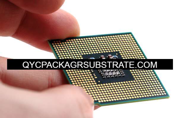
What is a MIS Package Substrate?
A MIS (Microtrace Integrated Substrate) package substrate is designed for high-density electronic packaging applications, especially in microelectronic devices like ICs (Integrated Circuits). It incorporates advanced technologies to achieve precise electrical connections between components while minimizing size and maximizing performance.
MIS substrates typically feature microtrace routing and micro-vias, allowing for dense interconnects and efficient heat dissipation. These substrates are crucial in modern electronics, where space constraints and performance demands are critical. They are manufactured using processes like thin-film deposition, etching, and bonding to ensure high reliability and performance under various operating conditions.
The design and production of MIS substrates involve detailed engineering to meet specific electrical, thermal, and mechanical requirements of the integrated circuits they support. They play a vital role in enabling smaller, more powerful electronic devices across industries ranging from consumer electronics to telecommunications and aerospace.
MIS Package Substrate Manufacturer
What are the MIS Package Substrate Design Guidelines?
Design guidelines for MIS (Microtrace Integrated Substrate) package substrates focus on achieving optimal performance, reliability, and manufacturability. Here are key considerations:
- Material Selection: Choose materials with excellent thermal conductivity, low coefficient of thermal expansion (CTE), and good electrical properties suitable for high-frequency signals.
- Layer Configuration: Optimize the number and configuration of substrate layers to minimize signal losses and maximize heat dissipation. Consider using micro-vias to achieve dense routing.
- Microtrace Routing: Implement controlled impedance and signal integrity techniques in microtrace routing to ensure reliable signal transmission and minimize electromagnetic interference (EMI).
- Via Design:Use micro-vias and buried vias to achieve high-density interconnects without compromising signal integrity. Ensure proper via aspect ratios for reliable plating and filling.
- Thermal Management: Incorporate thermal vias and thermal pads strategically to enhance heat dissipation and maintain component reliability under thermal stress.
- Dimensional Tolerances: Specify tight dimensional tolerances for critical features to ensure compatibility with assembly processes and alignment accuracy.
- Surface Finish: Select appropriate surface finishes (e.g., ENIG, OSP) to achieve good solderability and prevent oxidation, ensuring robust solder joints during assembly.
- Assembly Compatibility: Design for manufacturability (DFM) by considering assembly processes such as solder paste printing, component placement, and reflow soldering.
- Reliability Testing:Plan for reliability testing including thermal cycling, mechanical shock, and vibration tests to validate substrate performance under real-world conditions.
- Documentation and Communication: Provide comprehensive design documentation including layer stack-up, material specifications, and fabrication notes to facilitate smooth manufacturing and assembly processes.
Following these guidelines helps ensure that MIS package substrates meet the stringent requirements of high-performance electronic devices, enhancing reliability and enabling miniaturization in advanced applications.
What is the MIS Package Substrate Fabrication Process?
The fabrication process for MIS (Microtrace Integrated Substrate) package substrates involves several key steps to achieve the desired electrical, thermal, and mechanical properties:
- Substrate Material Preparation:Select and prepare substrate materials that meet the design requirements, including properties like thermal conductivity, dielectric constant, and coefficient of thermal expansion (CTE).
- Substrate Lamination: Layer the substrate materials according to the specified stack-up configuration. This process involves bonding layers together using heat and pressure to form a solid substrate with the desired electrical and mechanical properties.
- Drilling and Micro-via Formation: Drill holes for through vias and micro-vias using precision drilling equipment. Micro-vias are typically created using laser drilling or mechanical drilling with advanced control to achieve small diameters and high aspect ratios.
- Via Filling and Plating: Fill the drilled vias with conductive material (such as copper) to form electrical connections between different substrate layers. Electroplating is often used to deposit and build up the conductive layers inside the vias.
- Pattern Imaging: Apply a photosensitive resist material to the substrate surface and expose it to UV light through a photomask. This step defines the circuit pattern and locations for conductive traces and pads.
- Etching: Use chemical etching to remove the exposed areas of copper or other conductive materials, leaving behind the desired circuit traces and features. Precision etching ensures accurate trace widths and spacing according to design specifications.
- Surface Finish Application: Apply a surface finish to the substrate to enhance solderability and protect exposed copper surfaces from oxidation. Common surface finishes include Electroless Nickel Immersion Gold (ENIG) or Organic Solderability Preservative (OSP).
- Solder Mask Application: Apply solder mask over the substrate surface to insulate and protect the circuit traces, leaving openings (exposed pads) for solder connections to electronic components.
- Final Fabrication Steps: Complete the fabrication process by performing final inspections, testing for dimensional accuracy, and ensuring compliance with design specifications. This may include electrical testing to verify circuit continuity and functionality.
- Quality Assurance and Testing: Conduct rigorous quality checks and reliability testing, such as thermal cycling, mechanical stress tests, and electrical performance evaluations, to ensure the substrate meets performance requirements and reliability standards.
Overall, the fabrication of MIS package substrates requires precise control over material selection, manufacturing processes, and quality assurance to produce substrates that meet the demanding requirements of modern electronic devices.
How do you manufacture a MIS Package Substrate?
Manufacturing a MIS (Microtrace Integrated Substrate) package substrate involves a series of meticulous steps to ensure high performance and reliability:
- Material Selection: Choose substrate materials based on thermal conductivity, dielectric properties, and CTE to meet design requirements. Common materials include ceramics or high-performance laminates.
- Layer Stacking: Laminate substrate layers using heat and pressure to create a solid base with desired electrical and mechanical properties. Ensure alignment and bonding integrity.
- Via Formation:Drill holes for through vias and micro-vias using precision equipment. Micro-vias are typically formed using laser drilling for small diameters and high aspect ratios.
- Via Filling and Plating: Fill vias with conductive material (e.g., copper) using electroplating to establish electrical connections between substrate layers. Control plating thickness for uniform conductivity.
- Circuit Patterning:Apply a photosensitive resist and expose to UV light through a mask to define circuit patterns. Develop and etch away exposed copper to form circuit traces with precise dimensions.
- Surface Finish Application: Apply surface finishes like ENIG or OSP to protect exposed copper and ensure solderability. Control surface roughness and thickness to meet assembly requirements.
- Solder Mask Application: Coat substrate with solder mask and cure to insulate circuit traces, leaving openings for component pads. Ensure precise registration with circuit features.
- Final Inspection: Perform visual inspection, dimensional checks, and electrical testing to verify circuit continuity and integrity. Use automated inspection tools for accuracy.
- Quality Assurance: Conduct reliability tests such as thermal cycling and mechanical stress tests to assess substrate performance under operational conditions.
- Packaging and Shipping: Package substrates in protective materials to prevent damage during transit. Ensure proper documentation and traceability of manufacturing processes.
By following these steps with attention to detail and quality control, manufacturers can produce MIS package substrates that meet stringent requirements for high-density interconnects and reliable electronic performance.
How much should a MIS Package Substrate cost?
The cost of a MIS (Microtrace Integrated Substrate) package substrate can vary significantly based on several factors:
- Complexity and Design Requirements: More complex designs with higher layer counts, finer trace widths, and tighter tolerances generally increase manufacturing costs.
- Material Selection: The type and quality of substrate materials (e.g., ceramics, high-performance laminates) impact costs. Materials with specific thermal conductivity or dielectric properties may be more expensive.
- Manufacturing Processes: Techniques such as laser drilling for micro-vias, precise etching for fine traces, and advanced surface finishes contribute to manufacturing costs.
- Size and Quantity: Larger substrates or higher volumes typically reduce per-unit costs due to economies of scale in production.
- Additional Features: Optional features like special surface finishes (e.g., ENIG), controlled impedance, and thermal management enhancements can add to the cost.
- Supplier and Geographic Location: Costs may vary based on the supplier’s capabilities, location, and currency fluctuations.
To provide a rough estimate, prices for MIS package substrates can range from a few dollars per square inch for simpler designs to tens of dollars per square inch or more for complex, high-performance substrates. Exact pricing would require detailed specifications and possibly contacting suppliers for quotes based on specific project requirements.
What is MIS Package Substrate base material?
The base materials used for MIS (Microtrace Integrated Substrate) package substrates typically include advanced ceramics or high-performance laminates. These materials are chosen for their specific properties that are critical for electronic packaging applications:
- Advanced Ceramics: Ceramics such as alumina (Al₂O₃) or aluminum nitride (AlN) are known for their excellent thermal conductivity, high electrical insulation, and mechanical strength. These properties make them suitable for applications requiring efficient heat dissipation and reliable electrical performance.
- High-Performance Laminates: These laminates are engineered to provide a balance of electrical properties (dielectric constant, loss tangent), thermal management capabilities, and mechanical stability. They may include materials like polyimide-based laminates, PTFE-based laminates (e.g., Rogers materials), or other specialty substrates tailored for specific performance requirements.
The choice between ceramics and laminates depends on factors such as thermal management needs, signal integrity requirements, and mechanical constraints of the application. Advanced ceramics are often preferred in high-power applications where heat dissipation is critical, while high-performance laminates offer flexibility and compatibility with standard PCB manufacturing processes.
Each substrate material is selected based on its ability to meet the design specifications for thermal conductivity, dielectric properties, CTE (Coefficient of Thermal Expansion), and overall reliability in the intended electronic packaging environment.
Which company makes MIS Package Substrates?
Currently, there are many companies producing MIS (Microtrace Integrated Substrate) package substrates, covering multiple leading manufacturers in the electronics manufacturing field. These companies have deep expertise and rich experience in material selection, process technology, and market demand.
- Rogers Corporation, USA: Rogers Corporation is renowned for its high-performance electronic materials, including those used in microelectronic packaging. Their materials such as the Rogers RO4000 series and RO3000 series are widely used in microelectronic packaging for high-frequency and high-speed circuits.
- Shin-Etsu Chemical Co., Ltd., Japan: Shin-Etsu Chemical Co., Ltd. excels in silicon-based materials, packaging materials, and electronic materials. Their products are extensively used in semiconductor packaging and microelectronic packaging.
- Fischer Elektronik GmbH & Co. KG, Germany: Fischer Elektronik focuses on thermal management technology and packaging solutions. They offer various types of heat sinks, packaging bases, and special radiators, providing efficient thermal performance for electronic products.
- Shengli Electronics Co., Ltd., Shenzhen, China: Shengli Electronics is one of the leading electronic manufacturing service providers in China, specializing in high-density interconnect printed circuit boards (HDI PCBs) and microelectronic packaging solutions. Their products include various complex printed circuit boards and microelectronic packaging, widely used in communications, consumer electronics, and industrial control fields.
Our Company: We specialize in the production and supply of high-performance MIS Package Substrates (Microtrace Integrated Substrate) and other microelectronic packaging solutions. We have advanced production equipment and a skilled technical team capable of customizing various complex packaging substrates according to customer-specific requirements.
Our production capabilities encompass a variety of material choices, including advanced ceramics and high-performance laminates, to meet various technical requirements from thermal management to high-frequency signal integrity. We prioritize product quality and technological innovation, ensuring each product meets customers’ expected performance criteria through rigorous quality control and reliability testing.
If you are interested in our offerings of MIS Package Substrates or other microelectronic packaging products, or if you have specific requirements, please feel free to contact us. We are committed to providing high-quality products and professional technical support to help you achieve project success and market competitiveness.
What are the 7 qualities of good customer service?
Good customer service is characterized by several key qualities that contribute to customer satisfaction and loyalty:
- Responsiveness:Customers appreciate timely responses to their inquiries, whether through phone calls, emails, or in-person interactions. Prompt assistance shows respect for their time and urgency.
- Empathy: Showing empathy involves understanding and acknowledging the customer’s emotions, concerns, and needs. It helps build rapport and trust, demonstrating genuine care for their experience.
- Professionalism: Maintaining professionalism in demeanor, communication, and problem-solving instills confidence in customers. It includes being courteous, respectful, and knowledgeable in addressing their issues.
- Knowledgeability: Having adequate product knowledge and expertise allows customer service representatives to provide accurate information and effective solutions. This builds credibility and enhances the customer’s experience.
- Accessibility: Ensuring easy access to customer support channels and assistance is crucial. This includes offering multiple contact options, clear instructions, and availability during business hours or through self-service options.
- Reliability:Consistently delivering on promises and commitments fosters trust. Reliable service includes following up on issues, keeping customers informed, and resolving problems efficiently.
- Personalization: Tailoring interactions to meet individual customer needs and preferences enhances satisfaction. This can involve remembering previous interactions, offering personalized recommendations, or adapting communication styles.
By prioritizing these qualities, businesses can cultivate positive customer relationships, improve retention rates, and differentiate themselves in competitive markets.
FAQs
What are MIS package substrates?
MIS package substrates are advanced electronic packaging solutions designed for high-density interconnects in microelectronic devices. They incorporate technologies like micro-vias and precise circuit routing for efficient signal transmission and heat dissipation.
What are the advantages of MIS package substrates?
MIS substrates offer advantages such as high thermal conductivity, excellent electrical performance, and the ability to support complex circuit designs with fine traces and vias. They are crucial for miniaturization and performance enhancement in electronic devices.
Which industries use MIS package substrates?
MIS substrates are used in industries requiring high-performance electronics, including telecommunications, aerospace, automotive, and consumer electronics. They support applications ranging from high-speed data transmission to power electronics.
How are MIS package substrates manufactured?
The manufacturing process involves substrate material selection (typically ceramics or high-performance laminates), layer stacking, via formation (including micro-vias), circuit patterning, and surface finishing. Quality control and testing ensure reliability and performance.
What factors affect the cost of MIS package substrates?
Cost factors include substrate complexity, material selection, manufacturing processes (e.g., laser drilling), size, and volume. Higher performance requirements and specialized features may increase production costs.
Where can I find suppliers of MIS package substrates?
Suppliers include global manufacturers specializing in electronic materials and packaging solutions. Companies like Rogers Corporation, Shin-Etsu Chemical Co., Ltd., and local electronics manufacturers provide MIS substrates tailored to specific industry needs.