
Mixed dielectric PCB manufacturing
Mixed dielectric PCB manufacturing, FR4/High speed/high frequency Mixed dielectric PCB manufacturer. Professional PCB production company. High quality and fast lead time.
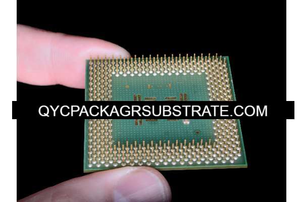
Mixed Dielectric PCBs are advanced printed circuit boards that integrate multiple types of dielectric materials within their construction. Unlike traditional PCBs that use a single dielectric material throughout, Mixed Dielectric PCBs strategically employ different dielectric materials in various regions of the board to optimize performance. By tailoring the electrical properties of each area, these PCBs offer improved signal integrity, reduced crosstalk, better thermal management, and enhanced reliability. Common dielectric materials used in Mixed Dielectric PCBs include FR-4, Rogers materials, Teflon (PTFE), polyimide, and metal core substrates. These materials vary in terms of dielectric constant, loss tangent, and other electrical properties, allowing designers to achieve precise control over the PCB’s electrical characteristics. Mixed Dielectric PCBs find applications in high-frequency and high-speed electronics, such as telecommunications, aerospace, automotive, and consumer electronics, where demanding performance requirements must be met.
What is a Mixed Dielectric PCB?
Mixed dielectric PCB manufacturing.High speed and high frequency material packaging substrate manufacturing. Advanced packaging substrate production process and technology
A Mixed Dielectric PCB (Printed Circuit Board) refers to a circuit board design that incorporates multiple types of dielectric materials within its construction. Dielectric materials are non-conductive substances used to insulate conductive components on a PCB, preventing electrical shorts and interference.
In a Mixed Dielectric PCB, different regions of the board may use different dielectric materials based on the specific requirements of those areas. This approach allows engineers to tailor the electrical properties of the PCB to suit different needs within the same board. For example, some regions might require higher insulation resistance, while others may need lower signal loss or better impedance matching.
By utilizing different dielectric materials in different areas, Mixed Dielectric PCBs can achieve a variety of goals, such as improved signal integrity, reduced crosstalk, better thermal management, or enhanced reliability. This design strategy is particularly common in high-frequency and high-speed applications where precise control over electrical characteristics is crucial for optimal performance.
Mixed dielectric PCB manufacturing
What are the Mixed Dielectric PCB Design Guidelines?
Designing a Mixed Dielectric PCB involves several considerations and guidelines to ensure optimal performance and reliability. Here are some key guidelines:
- Dielectric Material Selection: Carefully select dielectric materials based on their electrical properties, such as permittivity (dielectric constant), loss tangent, and temperature stability. Different regions of the PCB may require different dielectric materials to meet specific performance requirements.
- Layer Stackup Design: Plan the layer stackup to accommodate different dielectric materials. Place layers with similar dielectric constants close to each other to minimize signal distortion and impedance mismatches.
- Signal Integrity: Maintain signal integrity by minimizing signal loss, crosstalk, and impedance variations. Ensure that transitions between different dielectric materials are smooth to reduce reflections and signal degradation.
- Impedance Control: Control impedance by adjusting trace width, spacing, and layer thickness based on the dielectric properties of each region. Use impedance calculators or field solvers to accurately calculate and verify impedance values.
- Thermal Management: Consider thermal effects of different dielectric materials and their dissipation capabilities. Ensure that heat generated by components or high-power traces is effectively dissipated to prevent overheating and reliability issues.
- Manufacturability: Ensure that the chosen dielectric materials can be reliably manufactured and processed during PCB fabrication. Verify compatibility with fabrication processes such as lamination, drilling, and plating.
- Testing and Validation: Perform thorough testing and validation to verify the performance of the Mixed Dielectric PCB design. Use signal integrity analysis, impedance testing, and thermal testing to identify and address any issues before mass production.
- Documentation: Document the selection of dielectric materials, layer stackup design, impedance profiles, and other design parameters for future reference and troubleshooting.
By following these guidelines, designers can effectively design Mixed Dielectric PCBs that meet the required performance criteria and ensure robust operation in diverse applications.
What is the Mixed Dielectric PCB Fabrication Process?
The fabrication process for a Mixed Dielectric PCB is similar to that of a standard PCB but requires additional considerations due to the use of multiple dielectric materials. Here are the general steps involved in the fabrication process:
- Design Preparation: Begin with the PCB design, specifying the regions where different dielectric materials will be used. Design the layer stackup accordingly, ensuring proper alignment and registration of different materials.
- Material Selection: Select the appropriate dielectric materials based on their electrical properties, thermal characteristics, and compatibility with fabrication processes. Ensure that the chosen materials can be effectively bonded together during lamination.
- Substrate Preparation: Prepare the substrate materials, typically FR-4 or other rigid substrates, by cleaning and surface treatment to promote adhesion of copper and dielectric layers.
- Copper Cladding: Apply copper foil to the substrate surfaces using an adhesive or heat-activated bonding process. Etch the copper to create the desired circuit pattern using photolithography and chemical etching techniques.
- Dielectric Layer Preparation: Apply the different dielectric materials to the substrate, either as pre-preg sheets or liquid resins, depending on the fabrication method. Ensure proper alignment and registration between layers.
- Lamination: Stack the prepared layers together, including copper layers and dielectric materials, and subject them to heat and pressure in a lamination press. This process bonds the layers together to form a solid composite structure.
- Drilling: Drill holes for vias and component mounting pads using precision drilling machines. Control the drilling process carefully to avoid delamination or damage to the layered structure.
- Plating: Plate the drilled holes with copper to form vias, connecting different layers of the PCB. This can be done using electroplating or other metallization techniques.
- Surface Finishing: Apply surface finishes such as solder mask and surface plating to protect the copper traces and provide solderability for component attachment.
- Etching and Inspection: Etch away any excess copper and perform thorough inspection of the PCB for defects, ensuring that the design specifications are met.
- Testing and Quality Assurance: Conduct electrical testing, impedance testing, and other quality checks to verify the performance and reliability of the fabricated PCB.
- Final Assembly: Complete the PCB assembly by mounting components onto the board using soldering or other attachment methods.
- Testing and Validation: Perform final testing and validation to ensure that the assembled PCB meets the required specifications and functions correctly.
Throughout the fabrication process, it’s essential to maintain strict control over process parameters, such as temperature, pressure, and material handling, to achieve uniformity and consistency in the finished PCB. Additionally, documentation of the fabrication steps and quality control measures is crucial for traceability and troubleshooting.
How do you Manufacture a Mixed Dielectric PCB?
Manufacturing a Mixed Dielectric PCB involves several key steps in the fabrication process. Here’s an overview of the typical manufacturing process:
- Design Preparation:
– Create the PCB design using a computer-aided design (CAD) software, considering the mixed dielectric requirements.
– Specify the regions where different dielectric materials will be used and define layer stackup accordingly.
- Material Selection:
– Select appropriate dielectric materials based on their electrical properties and compatibility with the fabrication process.
– Ensure compatibility between different materials to prevent delamination or other issues during manufacturing.
- Preparation of Substrate Materials:
– Cut or shear the substrate materials (usually fiberglass or other composite materials) into the required sizes and shapes according to the PCB design.
- Layer Lamination:
– Prepreg layers, which are layers of resin-saturated fiberglass, are interleaved between the substrate layers.
– The layers are then stacked together in the desired sequence, incorporating the different dielectric materials as specified in the design.
– The stack is subjected to heat and pressure in a lamination press, bonding the layers together to form a solid panel.
- Drilling and Copper Plating:
– Holes for vias and component leads are drilled into the laminated panel using precision drilling machines.
– Copper foil is bonded to both sides of the panel, and the panel undergoes a process of copper plating to create the conductive traces and vias.
- Circuit Patterning:
– Apply a layer of photosensitive material (photoresist) onto the copper surfaces.
– Expose the photoresist to UV light through a photomask containing the circuit pattern, creating a photochemical reaction that defines the copper traces and pads.
– Develop and etch away the unexposed photoresist and unwanted copper, leaving behind the desired circuit pattern.
- Surface Finishing:
– Apply surface finish to protect the exposed copper traces and provide solderability.
– Common surface finishes include HASL (Hot Air Solder Leveling), ENIG (Electroless Nickel Immersion Gold), or OSP (Organic Solderability Preservatives).
- Final Processing:
– Rout the PCB to remove excess material and define the board outline.
– Perform electrical testing to ensure the integrity and functionality of the manufactured PCB.
– Optionally, apply solder mask and silkscreen for insulation and component identification.
- Quality Control and Inspection:
– Conduct visual inspection and electrical testing to verify the quality and reliability of the manufactured PCB.
– Ensure that the dimensions, tolerances, and electrical characteristics meet the design specifications.
- Packaging and Shipping:
– Package the finished PCBs according to the customer’s requirements and prepare them for shipping or further assembly processes.
Throughout the manufacturing process, strict quality control measures are implemented to ensure the consistency and reliability of the Mixed Dielectric PCBs. Any deviations or defects are identified and corrected to meet the desired specifications.
How Much Should a Mixed Dielectric PCB Cost?
The cost of a Mixed Dielectric PCB can vary significantly depending on various factors such as the complexity of the design, the size of the board, the number of layers, the types of materials used, and the quantities ordered. However, Mixed Dielectric PCBs typically tend to be more expensive than standard single-material PCBs due to the additional complexity involved in manufacturing and the higher cost of specialized dielectric materials.
Here are some key factors that can influence the cost of a Mixed Dielectric PCB:
- Design Complexity: The complexity of the PCB design, including the number of layers, the density of components, and the intricacy of the routing, can affect the manufacturing cost.
- Material Costs: The cost of dielectric materials used in the PCB, especially if they are specialized or high-performance materials, can significantly impact the overall cost.
- Manufacturing Processes: Additional manufacturing processes, such as controlled impedance routing, blind and buried vias, or sequential lamination, can increase production costs.
- Production Volume: Typically, larger production volumes lead to lower per-unit costs due to economies of scale. However, small batch orders or prototypes may incur higher costs per unit.
- Quality Requirements: Meeting stringent quality standards and testing requirements may require additional testing processes, which can contribute to the overall cost.
- Lead Time: Expedited production schedules or quick-turn services may come at a premium price compared to standard lead times.
To get an accurate cost estimate for a Mixed Dielectric PCB, it’s best to consult with PCB manufacturers or suppliers. They can provide detailed quotes based on the specific requirements of the project, including the design specifications, materials, quantities, and desired delivery schedule. Additionally, obtaining multiple quotes from different suppliers can help in finding the most cost-effective solution while meeting the required quality standards.
What is Mixed Dielectric PCB Base Material?
The base material of a Mixed Dielectric PCB refers to the substrate material upon which the conductive traces and components are built. This substrate provides mechanical support and insulation between the conductive layers of the PCB.
In a Mixed Dielectric PCB, the base material can vary depending on the specific requirements of the design and the regions where different dielectric materials are employed. Common base materials used in PCB fabrication include:
- FR-4 (Flame Retardant 4): FR-4 is the most widely used base material in PCB manufacturing due to its excellent electrical insulation properties, mechanical strength, and cost-effectiveness. It is composed of woven fiberglass cloth impregnated with epoxy resin.
- Rogers Materials: Rogers Corporation produces a range of high-performance laminates specifically designed for RF/microwave applications. These materials offer low dielectric loss, controlled impedance, and stable electrical properties over a wide frequency range. Examples include RO4000 series and RO3000 series laminates.
- Isola Materials: Isola is another major manufacturer of PCB laminates, offering a variety of materials suitable for high-speed digital and RF/microwave applications. Their materials include low-loss dielectrics such as IS620 and IS680.
- Teflon (Polytetrafluoroethylene, PTFE): Teflon-based materials are known for their low dielectric constant and low loss tangent, making them ideal for high-frequency applications. However, they are more expensive than FR-4 and may require specialized processing techniques.
- Polyimide: Polyimide-based substrates offer excellent thermal stability and flexibility, making them suitable for applications requiring high-temperature operation or flexible PCBs.
- Metal Core (MCPCB): Metal core PCBs use a metal substrate (typically aluminum or copper) as the base material instead of fiberglass. They are commonly used for thermal management applications where heat dissipation is critical.
For a Mixed Dielectric PCB, different regions of the board may utilize different base materials to accommodate the varying dielectric requirements. Careful selection of base materials is essential to ensure the desired electrical performance, mechanical stability, and reliability of the PCB design.
Which Company Makes Mixed Dielectric PCBs?
Many companies are capable of manufacturing Mixed Dielectric PCBs, but which companies produce this type of PCB may vary depending on market demand, technical capabilities, and production scale. Some well-known PCB manufacturers and suppliers may offer manufacturing services for Mixed Dielectric PCBs, including large electronic manufacturing services (EMS) companies, specialized PCB manufacturers, and some custom PCB manufacturers.
Just like our company, we have advanced production equipment and a skilled technical team capable of meeting the demands for Mixed Dielectric PCBs. With years of PCB manufacturing experience, we have a professional design and engineering team capable of providing customized solutions for Mixed Dielectric PCBs according to customer requirements. We prioritize quality and reliability, adhering to strict quality control standards to ensure high-quality PCB products are produced.
Our manufacturing process includes advanced processes such as lamination, drilling, circuit patterning, surface treatment, and more, capable of meeting the requirements of various complex PCB designs. We also offer comprehensive technical support and customer service to ensure timely communication and support throughout the project.
If you are looking for a reliable PCB manufacturer to produce Mixed Dielectric PCBs, our company can meet your needs. We are committed to providing high-quality products and excellent service, and we look forward to collaborating with you to create a better future.
What are the 7 Qualities of Good Customer Service?
Good customer service is essential for building strong customer relationships and fostering loyalty. Here are seven qualities that characterize excellent customer service:
- Responsiveness: Good customer service involves promptly addressing customer inquiries, concerns, and requests. Responding to customers in a timely manner demonstrates respect for their time and shows that their needs are valued.
- Empathy: Empathy is the ability to understand and relate to the emotions and experiences of customers. Empathetic customer service representatives listen actively, acknowledge customers’ feelings, and demonstrate compassion and understanding.
- Clear Communication: Effective communication is crucial in providing good customer service. Customer service representatives should communicate clearly and concisely, ensuring that customers understand information, instructions, and solutions provided.
- Knowledgeability: Knowledgeable customer service representatives possess a deep understanding of the products or services offered by the company. They are well-trained and equipped to answer questions, provide accurate information, and offer relevant solutions to customer issues.
- Problem-Solving Skills: Good customer service involves resolving customer problems and issues effectively. Customer service representatives should be skilled at identifying and addressing customer concerns, finding solutions to problems, and taking proactive steps to prevent future issues.
- Professionalism: Professionalism encompasses maintaining a courteous, respectful, and professional demeanor when interacting with customers. Customer service representatives should conduct themselves professionally at all times, regardless of the situation or customer’s behavior.
- Follow-Up: Following up with customers after resolving an issue or completing a transaction demonstrates commitment to customer satisfaction. Following up allows companies to ensure that customers are satisfied with the resolution, address any remaining concerns, and gather feedback for continuous improvement.
By embodying these qualities, businesses can deliver exceptional customer service experiences that leave customers satisfied, loyal, and likely to recommend the company to others.
FAQs (Frequently Asked Questions)
What is a Mixed Dielectric PCB?
A Mixed Dielectric PCB is a printed circuit board that incorporates multiple types of dielectric materials within its construction. These materials have different electrical properties and are strategically placed in different regions of the PCB to meet specific performance requirements.
What are the advantages of using Mixed Dielectric PCBs?
Mixed Dielectric PCBs offer several advantages, including improved signal integrity, reduced crosstalk, better thermal management, and enhanced reliability. By tailoring the dielectric materials to different areas of the board, designers can optimize the electrical characteristics for various applications.
What types of dielectric materials are used in Mixed Dielectric PCBs?
Common dielectric materials used in Mixed Dielectric PCBs include FR-4 (standard epoxy-glass laminate), Rogers materials (high-frequency laminates), Teflon (PTFE), polyimide, and metal core substrates. These materials vary in terms of dielectric constant, loss tangent, and other electrical properties.
What considerations should be made when designing Mixed Dielectric PCBs?
Designers must consider factors such as dielectric material selection, layer stackup design, signal integrity, impedance control, thermal management, manufacturability, and testing/validation. Each of these aspects plays a crucial role in optimizing the performance and reliability of the PCB.
What are some common applications of Mixed Dielectric PCBs?
Mixed Dielectric PCBs are commonly used in high-frequency and high-speed applications, such as telecommunications, aerospace, defense, automotive electronics, medical devices, and consumer electronics. They are also suitable for applications requiring precise control over electrical characteristics.
How can I ensure the quality of Mixed Dielectric PCBs?
To ensure the quality of Mixed Dielectric PCBs, it is essential to work with a reputable PCB manufacturer with experience in producing complex PCBs. Additionally, thorough testing and validation processes should be implemented to verify the performance and reliability of the PCB design.
Are there any specific design guidelines for Mixed Dielectric PCBs?
Yes, there are specific design guidelines for Mixed Dielectric PCBs, including considerations for material selection, layer stackup design, signal integrity, impedance control, thermal management, manufacturability, and testing/validation. Adhering to these guidelines is crucial for achieving optimal performance and reliability.