
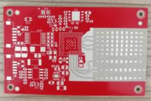
RO4350B PCB
RO4350B PCB Manufacturer, Rogers 4350B PCB and Ro4350B xed media laminating PCBs production. we offer Rogers Series material from 2 layer to 50 layers. High frequency PCB production factory.
RO4350B PCBs are high-performance printed circuit boards fabricated using RO4350B laminate material developed by Rogers Corporation. Renowned for their exceptional characteristics, RO4350B PCBs are specifically engineered for high-frequency applications demanding precise signal integrity and minimal loss. With a low dielectric constant (Dk) and dissipation factor (Df), these PCBs offer reliable signal transmission at microwave frequencies, ensuring optimal performance in telecommunications, aerospace, automotive radar systems, and satellite communications. Their excellent thermal conductivity aids in efficient heat dissipation, making them ideal for high-power applications. RO4350B PCBs also exhibit dimensional stability, maintaining their shape and integrity even under demanding conditions. Design considerations such as controlled impedance, proper grounding, and shielding are crucial to maximize the potential of RO4350B PCBs. Whether used in complex RF circuits or critical microwave devices, RO4350B PCBs deliver unparalleled performance, reliability, and longevity.
What is RO4350B PCB?
RO4350B is a type of high-frequency laminate material used in printed circuit boards (PCBs). It’s manufactured by Rogers Corporation, a leading supplier of advanced materials for various industries including electronics.
RO4350B is specifically designed for high-frequency applications where signal integrity, low loss, and thermal performance are critical factors. It has a dielectric constant (Dk) of approximately 3.48 and a dissipation factor (Df) of around 0.0037 at 10 GHz, making it suitable for microwave and RF applications.
PCBs made with RO4350B are commonly used in telecommunications, aerospace, automotive radar systems, satellite communications, and other high-frequency electronic devices where performance at microwave frequencies is essential.
What are the RO4350B PCB Design Guidelines?
Designing PCBs with RO4350B material requires attention to specific guidelines to ensure optimal performance at high frequencies. Here are some general design guidelines:
- Dielectric Constant (Dk) and Dissipation Factor (Df):Understand the dielectric constant and dissipation factor of RO4350B material at the frequencies of operation, as they can vary slightly with frequency.
- Trace Width and Spacing:Maintain appropriate trace widths and spacing to achieve the desired characteristic impedance (Z0). Use a controlled impedance design approach to ensure signal integrity.
- Ground Plane:Utilize solid ground planes to provide low impedance return paths for signal traces and to minimize electromagnetic interference (EMI). Maintain a continuous and uninterrupted ground plane beneath signal traces.
- Via Design:Use through-hole vias or blind/buried vias to transition between layers. Minimize via stubs to avoid signal reflections. Consider the use of back-drilling to remove via stubs in high-frequency applications.
- Component Placement:Optimize component placement to minimize trace lengths and reduce signal path impedance. Keep high-speed signal traces as short and direct as possible.
- Crosstalk Mitigation:Maintain appropriate spacing between signal traces to minimize crosstalk. Use differential signaling for high-speed data lines to improve noise immunity.
- Thermal Considerations:RO4350B has good thermal conductivity, but consider thermal management techniques such as heat sinks or thermal vias for components dissipating significant heat.
- EMC/EMI Compliance:Design PCB layouts to comply with electromagnetic compatibility (EMC) and electromagnetic interference (EMI) requirements. Proper grounding and shielding techniques are essential for minimizing emissions and susceptibility.
- Manufacturability:Ensure that the PCB design is manufacturable by considering fabrication and assembly constraints. Consult with your PCB manufacturer to validate the design for manufacturability.
- Simulation and Prototyping:Perform electromagnetic simulation using tools like HFSS, CST Microwave Studio, or ADS to validate the PCB design before prototyping. Prototype and test the PCB to verify its performance meets the desired specifications.
Following these guidelines can help ensure that PCBs designed with RO4350B material perform reliably in high-frequency applications. It’s also advisable to refer to Rogers Corporation’s specific design guidelines and application notes for RO4350B for more detailed information.
RO4350B PCB
What is the RO4350B PCB Fabrication Process?
The fabrication process for RO4350B PCBs follows standard PCB manufacturing procedures, with some considerations specific to the properties of RO4350B material. Here’s an overview of the typical fabrication process:
- Material Preparation:The fabrication process begins with the procurement of RO4350B laminate material in the desired thickness and copper foil type (typically rolled annealed copper). The laminate sheets are inspected for any defects before proceeding to the next steps.
- Preparation of Gerber Files:PCB designers create Gerber files containing the PCB layout, including the placement of copper traces, vias, pads, and other features. These files define the design of the PCB and are used by the manufacturer during fabrication.
- Prepreg and Core Layer Preparation:In multilayer PCBs, prepreg layers (layers of uncured resin with fiberglass reinforcement) and core layers (layers of cured resin with copper foil) are prepared according to the stackup design. RO4350B laminate material is typically used as core layers due to its high-frequency performance.
- Copper Cladding:Copper foil is laminated onto both sides of the RO4350B core layers using heat and pressure. The thickness of the copper foil is determined based on the required copper weight specified in the design.
- Laser Drilling:Holes for vias and through-hole components are drilled using laser drilling equipment. Laser drilling provides high precision and accuracy, essential for high-frequency applications.
- Through-Hole Plating:Through-holes are plated with conductive material (usually copper) to establish electrical connections between different layers of the PCB. This process is typically performed using electroplating techniques.
- Circuit Patterning: A layer of photoresist is applied to the copper-clad laminate, and the Gerber files are used to selectively expose the photoresist to UV light. The exposed areas are then developed, leaving behind the desired copper traces and features.
- Etching:The exposed copper is etched away using chemical processes, leaving behind the circuitry defined by the photoresist mask.
- Surface Finishing:Surface finish options such as HASL (Hot Air Solder Leveling), ENIG (Electroless Nickel Immersion Gold), or OSP (Organic Solderability Preservatives) may be applied to protect the exposed copper and improve solderability.
- Final Inspection and Testing:The fabricated PCB undergoes inspection to ensure that it meets the design specifications and quality standards. Electrical testing may be performed to verify continuity, impedance, and other electrical parameters.
- Routing and Profiling:Individual PCBs are routed out of the larger panel using milling or routing equipment. The edges are then smoothed, and any remaining copper burrs are removed.
- Quality Control and Packaging:The finished PCBs are subjected to final quality control checks before being packaged and prepared for shipment to the customer.
Throughout the fabrication process, it’s essential to follow best practices for handling and processing RO4350B material to ensure optimal performance in high-frequency applications. Additionally, collaboration between PCB designers and manufacturers is crucial to address any specific requirements or challenges associated with the material.
How do you manufacture an RO4350B PCB?
Manufacturing an RO4350B PCB involves several steps, from material selection to final testing. Here’s a detailed overview of the manufacturing process:
- Material Selection:Choose RO4350B laminate material from a trusted supplier like Rogers Corporation. Consider the required thickness, copper foil thickness, and any special characteristics needed for the application.
- Panel Preparation:Cut the RO4350B material into panels of the required size for the PCBs to be fabricated. Ensure that the panels are clean and free from contaminants.
- Preparation of Design Files: Design the PCB layout using CAD (Computer-Aided Design) software. Include all necessary elements such as traces, pads, vias, and components. Generate Gerber files, drill files, and other manufacturing data required for fabrication.
- Panelization:Arrange multiple PCB designs on a panel to maximize material usage and facilitate efficient manufacturing. Add fiducial marks and tooling holes for alignment during fabrication.
- Drilling:Use precision CNC drilling machines to drill holes for vias and component mounting pads according to the design specifications. Ensure accurate hole placement and size.
- Copper Deposition:Apply a thin layer of copper to the panel surfaces using an electroplating process. This step forms the conductive layers of the PCB.
- Circuit Patterning: Apply a layer of photoresist material to the copper-clad panels. Use photolithography techniques to expose the photoresist layer to UV light through a mask containing the PCB pattern. Develop the exposed photoresist to reveal the desired copper traces and pads.
- Etching:Immerse the panels in an etchant solution to remove the exposed copper and define the circuit traces and pads. Rinse the panels thoroughly to remove any remaining etchant.
- Surface Finish:Apply a surface finish to protect the exposed copper surfaces, improve solderability, and prevent oxidation. Common surface finishes for RO4350B PCBs include immersion gold, ENIG (Electroless Nickel Immersion Gold), and HASL (Hot Air Solder Leveling).
- Solder Mask Application: Apply a solder mask layer over the entire panel, leaving openings for solder pads and vias. Cure the solder mask to harden it and protect the copper traces from environmental factors and solder bridging during assembly.
- Silkscreen Printing: Print component outlines, reference designators, and other identification marks onto the PCB surface using silkscreen printing techniques. This information aids in assembly and inspection.
- Testing and Inspection:Conduct electrical testing to verify the continuity and integrity of the circuit traces. Perform visual inspection to check for defects such as misalignment, solder bridges, or missing features.
- Routing and Separation: If multiple PCBs are fabricated on a single panel, separate (route) them into individual boards using CNC routing machines. Clean the boards to remove any debris from the manufacturing process.
- Final Testing:Perform final electrical testing to ensure that the fabricated PCBs meet the specified performance criteria and functional requirements.
- Packaging and Shipping:Package the finished PCBs securely to prevent damage during transit. Label the packages with relevant information and ship them to the customer or assembly facility.
Throughout the manufacturing process, strict quality control measures should be implemented to ensure the reliability and performance of the RO4350B PCBs. It’s essential to follow the manufacturer’s recommended fabrication guidelines and best practices to achieve optimal results.
How much should an RO4350B PCB cost?
The cost of an RO4350B PCB can vary depending on several factors, including the size, complexity, quantity, and specifications of the PCB, as well as the chosen PCB manufacturer and any additional services required. Here are some factors that can influence the cost:
- Material Cost:RO4350B material is generally more expensive than standard FR-4 material due to its specialized characteristics and performance at high frequencies. The cost of the material will depend on the thickness and copper foil options chosen.
- Manufacturing Process:The fabrication process for RO4350B PCBs may require specialized equipment and techniques, particularly for high-frequency applications. This can impact the overall manufacturing cost.
- Design Complexity:PCBs with complex designs, high layer counts, dense component placement, and tight tolerances may require more time and effort to manufacture, resulting in higher costs.
- Quantity: PCB manufacturers often offer volume discounts for larger quantities. Ordering larger quantities of RO4350B PCBs can reduce the cost per unit.
- Additional Services:Additional services such as impedance control, gold plating, ENIG surface finish, and electrical testing can increase the cost of the PCB.
- Lead Time:Expedited manufacturing or quick-turn services may incur additional charges.
To get an accurate cost estimate for an RO4350B PCB, it’s best to consult with PCB manufacturers directly. Many manufacturers provide online quotation tools or allow customers to request a quote by providing detailed specifications and design files. By obtaining quotes from multiple manufacturers and comparing their offerings, you can find the most cost-effective solution for your project.
What is the RO4350B PCB base material?
RO4350B is a high-frequency laminate material used as the base material for PCBs. It is a proprietary product developed by Rogers Corporation, a leading manufacturer of advanced materials for various industries, including electronics.
RO4350B is composed of a woven fiberglass reinforcement material impregnated with a thermoset resin system. The resin system provides mechanical support and insulation properties, while the woven fiberglass reinforcement enhances dimensional stability and strength.
The key characteristics of RO4350B include:
- Low Dielectric Loss:RO4350B has a low dielectric loss, making it suitable for high-frequency applications where signal integrity is crucial.
- Stable Dielectric Constant:It offers a stable dielectric constant (Dk) over a wide frequency range, which is essential for maintaining consistent signal transmission characteristics.
- Excellent Thermal Conductivity:RO4350B has good thermal conductivity properties, allowing for efficient heat dissipation in high-power applications.
- Dimensional Stability:The woven fiberglass reinforcement provides excellent dimensional stability, ensuring that the PCB maintains its shape and integrity during fabrication and operation.
Overall, RO4350B is specifically engineered to meet the demanding requirements of high-frequency PCB applications, such as telecommunications, aerospace, automotive radar systems, and microwave devices. Its combination of low loss, stable Dk, and thermal performance makes it a preferred choice for engineers designing RF and microwave circuits.
Which company manufactures RO4350B PCBs?
RO4350B PCBs are typically manufactured by specialized PCB manufacturing companies, with Rogers Corporation being the producer of RO4350B material. This company is a leading manufacturer of advanced materials, focusing on providing high-performance material solutions for the electronics industry. RO4350B is a high-frequency laminate material produced by Rogers Corporation, featuring excellent performance characteristics suitable for various high-frequency applications such as microwave, RF, and millimeter-wave circuits.
Our company also manufactures RO4350B PCBs. As a professional PCB manufacturer, we have advanced equipment, an experienced team of engineers, and a stringent quality control system to meet the demands for high-performance PCBs. Our manufacturing processes adhere to industry standards, ensuring the production of RO4350B PCBs that meet specifications. We prioritize communication and collaboration with customers, aiming to deliver high-quality and reliable PCB solutions.
Our RO4350B PCB manufacturing process is carefully designed and optimized to ensure each step meets the highest quality standards. From material procurement to final inspection, we rigorously control every aspect to ensure customer satisfaction. We can customize RO4350B PCBs according to customer requirements, including different layer thicknesses, board thicknesses, process requirements, and surface treatment options.
As a global PCB manufacturer, we provide comprehensive services and support to customers. Whether you need high-frequency, high-performance RO4350B PCBs or other types of PCB solutions, we can meet your requirements. Feel free to contact us for more information about RO4350B PCB manufacturing, and we look forward to collaborating with you to drive the success of your project.
What are the 7 qualities of good customer service?
Good customer service is characterized by several key qualities that contribute to positive interactions and relationships with customers. Here are seven essential qualities:
- Empathy:Good customer service starts with empathy. Customer service representatives should be able to understand and relate to the needs, concerns, and emotions of customers. By empathizing with customers, representatives can provide more personalized and effective assistance.
- Patience:Patience is crucial in customer service, especially when dealing with complex issues or frustrated customers. Representatives should remain calm, listen attentively, and take the time to fully understand and address customer concerns without rushing or becoming frustrated themselves.
- Clear Communication:Clear and effective communication is essential for providing good customer service. Representatives should communicate clearly, using simple language and avoiding jargon or technical terms that customers may not understand. They should also actively listen to customers and ensure that they fully understand the issues and solutions being discussed.
- Problem-Solving Skills: Good customer service requires strong problem-solving skills. Representatives should be able to quickly and efficiently identify customer issues, analyze the root causes, and propose effective solutions. They should also be proactive in resolving problems and preventing future issues.
- Knowledgeability:Customers expect customer service representatives to be knowledgeable about the products or services offered by the company. Representatives should have a thorough understanding of the company’s offerings, policies, and procedures so that they can provide accurate information and assistance to customers.
- Reliability:Reliability is key to building trust and credibility with customers. Good customer service requires representatives to follow through on promises and commitments, meet deadlines, and provide consistent support to customers. Customers should feel confident that they can rely on the company to address their needs and concerns.
- Positive Attitude:A positive attitude can make a significant difference in customer interactions. Representatives should be friendly, approachable, and enthusiastic about helping customers. Even in challenging situations, maintaining a positive attitude can help diffuse tension and leave customers with a positive impression of the company.
By embodying these qualities, companies can deliver exceptional customer service experiences that foster customer loyalty, satisfaction, and advocacy.
FAQs
What is RO4350B PCB material?
RO4350B is a high-frequency laminate material manufactured by Rogers Corporation. It is specifically designed for high-frequency applications where signal integrity, low loss, and thermal performance are critical.
What are the key features of RO4350B PCBs?
RO4350B PCBs offer low dielectric loss, stable dielectric constant over a wide frequency range, excellent thermal conductivity, and dimensional stability. These characteristics make them suitable for applications such as telecommunications, aerospace, automotive radar systems, and microwave devices.
What are the advantages of using RO4350B PCBs?
The advantages of RO4350B PCBs include high performance at microwave frequencies, reliable signal transmission, low loss, and good thermal management properties. They are ideal for high-frequency applications where signal integrity is paramount.
How do RO4350B PCBs compare to standard FR-4 PCBs?
RO4350B PCBs offer superior performance at high frequencies compared to standard FR-4 PCBs. They have lower dielectric loss, better thermal conductivity, and more stable electrical properties, making them suitable for demanding RF and microwave applications.
What are some typical applications of RO4350B PCBs?
RO4350B PCBs are commonly used in telecommunications equipment, aerospace and defense systems, automotive radar systems, satellite communications, and other high-frequency electronic devices.
What are the design considerations for RO4350B PCBs?
Design considerations for RO4350B PCBs include maintaining controlled impedance, minimizing signal loss, optimizing thermal management, and ensuring proper grounding and shielding. Designers should also consider the specific requirements of their application and consult with the PCB manufacturer for guidance.
Where can I purchase RO4350B PCBs?
RO4350B PCBs can be purchased from specialized PCB manufacturers that offer high-frequency PCB fabrication services. It’s essential to choose a reputable manufacturer with experience in producing RO4350B PCBs to ensure quality and reliability.