
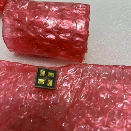
RT/duroid® 5880 Laminates PCB
RT/duroid® 5880 Laminates PCB manufacturing, Rogers series materials PCB Vendor, we offer Rogers PCBs from 2 layer to 30 layers, Characteristic: Microtrace, Small spacing, HDI Mixed dielectric layer, Cavity Rogers PCBs, Antenna, Radar, and other types Rogers PCBs producer.
RT/duroid® 5880 is a high-performance RF/microwave laminate material widely used in PCB (Printed Circuit Board) designs. This laminated board, based on a composite of polytetrafluoroethylene (PTFE) and ceramics, boasts excellent dielectric properties and stability, making it suitable for high-frequency and high-speed digital applications. RT/duroid® 5880’s material characteristics make it highly favored in fields such as microwave communications, radar systems, and antenna design. Its low loss and outstanding thermal stability make it an ideal choice for environments with frequent fluctuations. Additionally, the excellent machinability and reliability of RT/duroid® 5880 laminates ensure consistency and repeatability in designs, providing engineers with flexibility and convenience. In summary, RT/duroid® 5880 laminates play a crucial role in high-frequency electronic designs, offering reliable solutions for various applications.
What is a RT/duroid® 5880 Laminates PCB?
RT/duroid® 5880 is a type of high-frequency laminate commonly used in printed circuit boards (PCBs) for applications requiring excellent electrical performance at microwave frequencies. It is manufactured by Rogers Corporation, a leading supplier of advanced materials for electronics.
RT/duroid® 5880 laminates are known for their low dielectric constant (εr) and low loss tangent (Df), making them suitable for applications such as microwave antennas, radar systems, satellite communication systems, and high-frequency circuitry.
These laminates offer consistent electrical properties across a wide range of frequencies and temperatures, making them ideal for high-performance RF and microwave applications. They also provide good dimensional stability, mechanical strength, and ease of processing, which are essential characteristics for manufacturing high-frequency PCBs.
Overall, RT/duroid® 5880 laminates are valued for their reliability, high performance, and suitability for demanding applications in the telecommunications, aerospace, and defense industries, among others.
RT/duroid® 5880 Laminates PCB
What are the RT/duroid® 5880 Laminates PCB Design Guidelines?
Designing PCBs with RT/duroid® 5880 laminates requires careful consideration of its unique electrical and mechanical properties to achieve optimal performance. Here are some general guidelines for designing PCBs using RT/duroid® 5880 laminates:
- Transmission Line Design:RT/duroid® 5880 laminates are often used in high-frequency applications where transmission lines play a crucial role. Design transmission lines with controlled impedance to match the characteristic impedance of the laminate material. The specific impedance value will depend on the desired operating frequency and the stack-up of the PCB.
- Grounding: Proper grounding is essential for maintaining signal integrity and minimizing electromagnetic interference (EMI). Ensure a solid ground plane on one or both sides of the PCB, depending on the design requirements. Use vias to connect ground planes on different layers.
- Component Placement:Place components strategically to minimize signal path lengths and reduce parasitic capacitance and inductance. Group components according to their function and signal flow to optimize the layout.
- Thermal Management:Consider thermal management strategies to dissipate heat efficiently, especially in high-power applications. Thermal vias can help conduct heat away from heat-generating components to outer layers or heatsinks.
- Copper Thickness:RT/duroid® 5880 laminates are available in various copper thicknesses. Choose the appropriate copper thickness based on the current-carrying requirements and the desired level of signal attenuation.
- Via Design:Use high-frequency vias with low inductance and capacitance to minimize signal distortion and impedance mismatch. Employ techniques such as via stitching to enhance signal integrity and reduce ground bounce.
- Dielectric Thickness:The dielectric thickness between signal layers affects the characteristic impedance of transmission lines. Maintain consistent dielectric thickness throughout the PCB to ensure uniform signal propagation.
- Edge Coupling:Minimize edge coupling effects by maintaining a sufficient distance between signal traces and the PCB edge. This helps reduce signal reflections and improves signal integrity.
- Manufacturability:Consider manufacturability factors such as trace width and spacing, solder mask clearance, and minimum feature size to ensure the PCB can be manufactured accurately and reliably.
- Simulation and Testing:Use electromagnetic simulation tools to analyze signal integrity, impedance matching, and EMI issues during the design phase. Perform prototype testing to validate the performance of the PCB before mass production.
By following these guidelines and leveraging the unique properties of RT/duroid® 5880 laminates, you can design high-performance PCBs for demanding high-frequency applications.
RT/duroid® 5880 Laminates PCB
What is the RT/duroid® 5880 Laminates PCB Fabrication Process?
The fabrication process for PCBs using RT/duroid® 5880 laminates is similar to that of standard PCB fabrication processes, but with some specific considerations due to the properties of the laminate material. Here’s a general overview of the fabrication process:
- Design: Begin with the PCB design process using CAD software. Design the circuit layout, including component placement, routing, and signal traces, while adhering to the design guidelines for high-frequency applications and RT/duroid® 5880 laminates.
- Material Selection: Choose RT/duroid® 5880 laminates with the appropriate thickness and copper foil thickness based on the design requirements and performance specifications.
- Preparation of Substrate: Cut the RT/duroid® 5880 laminate material to the required size using precision cutting tools. Clean the substrate surface to remove any contaminants that could affect adhesion during lamination.
- Copper Cladding: Apply a thin layer of copper foil to one or both sides of the RT/duroid® 5880 laminate material using a lamination process. Ensure proper adhesion between the copper foil and the substrate surface.
- Photoresist Application: Apply a layer of photoresist material to the copper-clad laminate surface. This photoresist layer will be patterned to define the conductive traces and pads on the PCB.
- Exposure and Development: Use a photolithography process to expose the photoresist layer to UV light through a photomask, which contains the desired circuit pattern. Develop the exposed photoresist to remove the unexposed areas, leaving behind the patterned resist mask.
- Etching: Use chemical etchants, typically based on ferric chloride or ammonium persulfate, to selectively remove the exposed copper from the laminate surface, leaving behind the desired conductive traces and pads defined by the photoresist mask.
- Strip and Clean: Remove the remaining photoresist and etching residues from the PCB surface using appropriate stripping and cleaning solutions. Thoroughly rinse the PCB to ensure all contaminants are removed.
- Drilling: Drill holes for through-hole components and vias using precision drilling equipment. Ensure accurate hole placement and size to meet the design specifications.
- Plating: Plate the drilled holes with conductive material, typically copper, to provide electrical continuity between layers and facilitate component soldering. This process may involve electroless or electrolytic plating techniques.
- Solder Mask Application: Apply a solder mask layer over the PCB surface, leaving exposed only the areas where soldering is required, such as component pads and vias. Cure the solder mask to harden it and protect the underlying copper traces.
- Surface Finish: Apply a surface finish to protect the exposed copper surfaces from oxidation and facilitate soldering during assembly. Common surface finishes include HASL (Hot Air Solder Leveling), ENIG (Electroless Nickel Immersion Gold), and OSP (Organic Solderability Preservative).
- Silkscreen Printing: Optionally, apply silkscreen printing for component markings, reference designators, and other identification information on the PCB surface.
- Testing and Inspection: Perform electrical testing and visual inspection to ensure the fabricated PCB meets the design specifications and quality standards.
- Final Finishing: Cut the individual PCBs from the larger panel, if necessary, and perform any final finishing processes such as edge profiling or chamfering.
Following these steps, PCBs using RT/duroid® 5880 laminates can be fabricated with precision and reliability, suitable for high-frequency applications requiring excellent electrical performance.
How do you manufacture a RT/duroid® 5880 Laminates PCB?
Manufacturing a PCB using RT/duroid® 5880 laminates involves several steps, including material preparation, circuit layout design, fabrication, and assembly. Here’s an overview of the manufacturing process:
- Material Selection: Choose RT/duroid® 5880 laminates with the appropriate thickness and copper foil weight based on the design requirements and performance specifications. These laminates are typically supplied in sheet form and may have copper foil bonded to one or both sides.
- Preparation of Substrate: Cut the RT/duroid® 5880 laminate material to the desired dimensions using precision cutting tools. Clean the substrate surface to remove any contaminants that could affect adhesion during lamination.
- Copper Cladding: If necessary, laminate copper foil to one or both sides of the RT/duroid® 5880 substrate using heat and pressure. Ensure proper bonding between the copper foil and the substrate surface to achieve good electrical conductivity.
- Circuit Layout Design: Use computer-aided design (CAD) software to create the circuit layout, including component placement, routing, and signal traces. Follow design guidelines for high-frequency applications and RT/duroid® 5880 laminates to optimize performance and signal integrity.
- Artwork Generation: Generate the artwork for the PCB layout, including the conductor pattern, component pads, and other features, based on the design layout created in the CAD software.
- Photolithography: Transfer the artwork onto a photomask, which contains the desired circuit pattern, using a photolithography process. This involves coating the substrate with a photoresist material, exposing it to UV light through the photomask, and developing the exposed resist to create the patterned mask.
- Etching: Use chemical etchants, such as ferric chloride or ammonium persulfate, to selectively remove the exposed copper from the substrate surface, leaving behind the desired conductor traces and pads defined by the photoresist mask.
- Strip and Clean: Remove the remaining photoresist and etching residues from the PCB surface using appropriate stripping and cleaning solutions. Thoroughly rinse the PCB to ensure all contaminants are removed.
- Drilling: Drill holes for through-hole components and vias using precision drilling equipment. Ensure accurate hole placement and size to meet the design specifications.
- Plating: Plate the drilled holes with conductive material, typically copper, to provide electrical continuity between layers and facilitate component soldering. This may involve electroless or electrolytic plating techniques.
- Solder Mask Application: Apply a solder mask layer over the PCB surface, leaving exposed only the areas where soldering is required, such as component pads and vias. Cure the solder mask to harden it and protect the underlying copper traces.
- Surface Finish: Apply a surface finish to protect the exposed copper surfaces from oxidation and facilitate soldering during assembly. Common surface finishes include HASL (Hot Air Solder Leveling), ENIG (Electroless Nickel Immersion Gold), and OSP (Organic Solderability Preservative).
- Silkscreen Printing: Optionally, apply silkscreen printing for component markings, reference designators, and other identification information on the PCB surface.
- Testing and Inspection: Perform electrical testing and visual inspection to ensure the fabricated PCB meets the design specifications and quality standards.
- Final Finishing: Cut the individual PCBs from the larger panel, if necessary, and perform any final finishing processes such as edge profiling or chamfering.
Following these steps, you can manufacture high-quality PCBs using RT/duroid® 5880 laminates suitable for various high-frequency applications.
How much should a RT/duroid® 5880 Laminates PCB cost?
The cost of a PCB using RT/duroid® 5880 laminates can vary significantly depending on various factors such as:
- Board Size: Larger boards typically cost more due to the increased material and manufacturing expenses.
- Layer Count: PCBs with more layers require more material and complex manufacturing processes, leading to higher costs.
- Material Thickness: Thicker laminates may cost more than thinner ones due to the increased material usage.
- Copper Weight: Heavier copper foils (measured in ounces per square foot) can increase material costs.
- Complexity of Design: PCBs with intricate layouts, fine traces, and tight tolerances may require more labor and specialized equipment, resulting in higher costs.
- Surface Finish: Different surface finishes such as HASL, ENIG, or OSP have varying costs associated with their application processes.
- Quantity: Larger production quantities often result in lower per-unit costs due to economies of scale.
- Turnaround Time: Expedited manufacturing services typically come at a premium compared to standard lead times.
To get an accurate cost estimate for a PCB using RT/duroid® 5880 laminates, it’s best to consult with PCB manufacturers or suppliers. They can provide quotes based on your specific design requirements, quantities, and desired lead times. Additionally, online PCB cost calculators provided by some manufacturers can give you a rough estimate based on your design parameters.
What is RT/duroid® 5880 Laminates PCB base material?
RT/duroid® 5880 laminates are composed of a high-performance thermoset composite material. The base material typically consists of a woven fiberglass reinforcement impregnated with a polytetrafluoroethylene (PTFE) composite. PTFE is a type of synthetic fluoropolymer known for its excellent electrical insulation properties, low dielectric constant, and low loss tangent at high frequencies.
The woven fiberglass reinforcement provides mechanical strength and dimensional stability to the laminate, while the PTFE resin matrix offers exceptional electrical properties. The combination of these materials results in a substrate with consistent electrical performance across a wide range of frequencies, making it well-suited for high-frequency RF and microwave applications.
Additionally, RT/duroid® 5880 laminates may have one or both sides clad with thin copper foil layers. These copper foils provide the conductive pathways for circuit traces and component connections on the PCB, while the RT/duroid® substrate acts as the dielectric material separating the conductive layers.
Overall, the combination of woven fiberglass reinforcement and PTFE resin in RT/duroid® 5880 laminates creates a high-performance substrate with excellent electrical properties, mechanical stability, and reliability for demanding RF and microwave applications.
Which company makes RT/duroid® 5880 Laminates PCB?
RT/duroid® 5880 is one of the high-performance laminate series produced by Rogers Corporation. Rogers Corporation is a globally leading manufacturer of high-performance materials, specializing in providing various advanced material solutions for electronics, telecommunications, automotive, aerospace, and other industries. RT/duroid® 5880 is a specially designed laminate material to meet the needs of high-frequency applications, characterized by its excellent electrical performance and stability.
As a PCB manufacturing company, we have advanced production equipment and a skilled technical team capable of producing various types of PCBs, including high-frequency circuit boards using RT/duroid® 5880 material. We prioritize quality control, employing strict production processes and inspection standards to ensure that each PCB meets customer requirements and industry standards.
Our production process includes material preparation, lamination, chemical processing, photolithography, drilling, plating, printing, assembly, and more. With an experienced team of engineers, we can provide customized solutions tailored to customer design requirements, along with technical support and consulting services.
With PCBs manufactured by our company using RT/duroid® 5880 laminates, customers can expect excellent high-frequency performance and stable electrical characteristics suitable for various applications such as radar systems, microwave communication, antennas, and more. We are committed to providing customers with high-quality, reliable products and services to meet their demands for high-performance PCBs.
What are the 7 qualities of good customer service?
Good customer service is essential for building strong relationships with customers and ensuring satisfaction. Here are seven qualities that contribute to effective customer service:
- Responsiveness: A key aspect of good customer service is being responsive to customer inquiries, concerns, and requests in a timely manner. This includes promptly answering phone calls, replying to emails, and addressing customer needs promptly.
- Empathy: Empathy involves understanding and acknowledging the customer’s perspective, feelings, and needs. It’s important for customer service representatives to listen actively, show compassion, and demonstrate understanding, even when dealing with challenging situations.
- Clarity and Communication: Clear communication is vital for providing good customer service. Customer service representatives should communicate clearly and effectively, using language that is easy to understand and avoiding jargon. They should also provide accurate information and instructions to assist customers effectively.
- Problem-solving Skills: Good customer service involves the ability to effectively resolve customer issues and problems. Customer service representatives should be skilled at identifying the root cause of problems, offering solutions, and taking appropriate action to address customer concerns.
- Professionalism:Professionalism is important in all customer interactions. Customer service representatives should maintain a positive attitude, remain calm and composed, and treat customers with respect and courtesy at all times, regardless of the situation.
- Adaptability: In a dynamic environment, customer service representatives need to be adaptable and flexible. They should be able to quickly adjust to changing circumstances, handle unexpected challenges, and accommodate customer needs effectively.
- Follow-up and Follow-through: Good customer service doesn’t end with the initial interaction. It’s important to follow up with customers to ensure that their issues have been resolved satisfactorily and to address any additional concerns they may have. Following through on commitments and promises demonstrates reliability and builds trust with customers.
By embodying these qualities, businesses can deliver exceptional customer service experiences that foster loyalty, satisfaction, and positive word-of-mouth recommendations.
FAQs
What is RT/duroid® 5880 laminate?
RT/duroid® 5880 is a high-frequency laminate material manufactured by Rogers Corporation. It is known for its excellent electrical performance and is commonly used in PCBs for high-frequency applications.
What are the key characteristics of RT/duroid® 5880 laminates?
RT/duroid® 5880 laminates offer low dielectric constant (εr), low loss tangent (Df), and consistent electrical properties across a wide range of frequencies. They also provide good dimensional stability, mechanical strength, and ease of processing.
What are the typical applications of RT/duroid® 5880 laminates PCBs?
RT/duroid® 5880 laminates are used in various high-frequency applications, including microwave antennas, radar systems, satellite communication systems, RF/microwave circuits, and other demanding electronic systems requiring excellent electrical performance.
What are the advantages of using RT/duroid® 5880 laminates?
The advantages of RT/duroid® 5880 laminates include low signal loss, minimal dielectric absorption, high thermal conductivity, and good chemical resistance. These properties make them ideal for high-performance RF and microwave applications.
How does RT/duroid® 5880 compare to other laminates?
Compared to other laminates, RT/duroid® 5880 offers superior electrical performance at high frequencies, making it a preferred choice for critical applications where signal integrity is paramount.
What design considerations should be taken into account when using RT/duroid® 5880 laminates?
Design considerations include controlled impedance matching, proper grounding techniques, thermal management, transmission line design, and component placement to optimize performance and signal integrity.